This thread has been locked.

If you have a related question, please click the "Ask a related question" button in the top right corner. The newly created question will be automatically linked to this question.

UCC28780: Late PWML due to incomplete resonance swing

Part Number: UCC28780

I have my supply going, but timing and resonance seem to be off or drifting.  In ABM burst mode I typically see a couple good switching cycles and then I start to see the switch node voltage not dropping to zero after PWMH goes low.  This causes the next PWML to be late and to miss zero-voltage switching. I am operating with SET = 1 which is normally used for Si FET switches, but my high-voltage GaN switches have large output capacitance so SET = 0 switches too quickly.

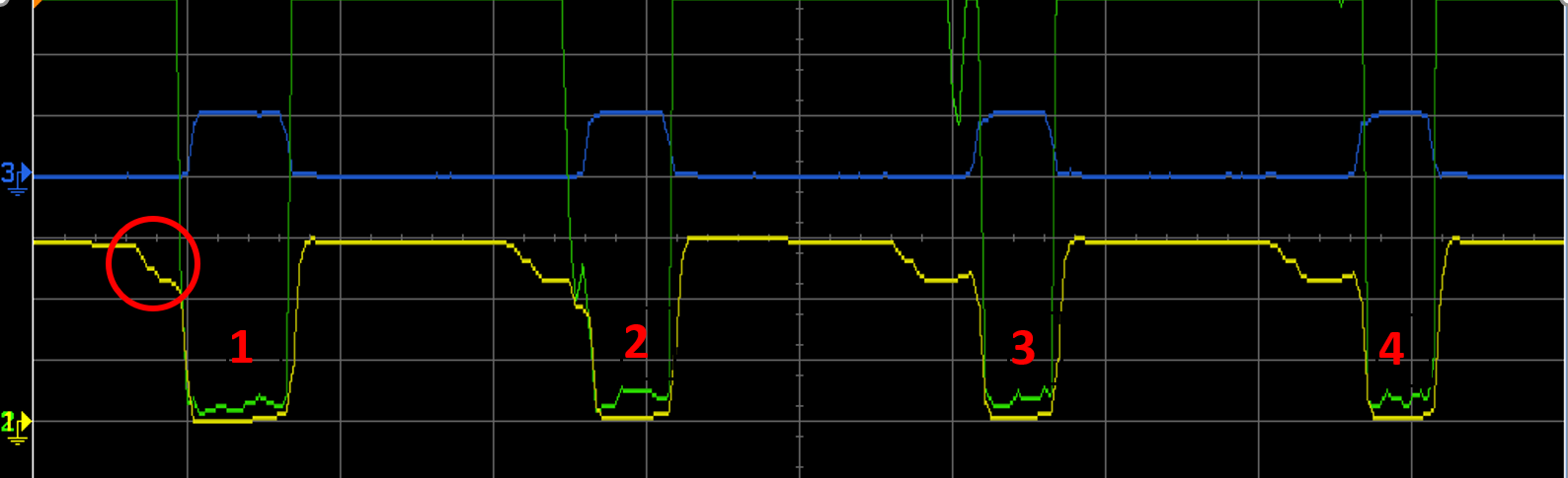
The traces below are yellow = SWS controller input at 2 V/div, green = high voltage switch node, captured at 100 V/div and zoomed in to 20 V/div with high-res capture, and blue = PWML at 5V/div.  Cycle 1 is normal, 2 is marginal, and 3 and 4 show the switch node voltage not reaching zero and late PWMLs.  The upper dotted line cursor is 9V, the SWT threshold to generate a PWML pulse.  You can see that SWT doesn't reach this threshold in pulses 3 and 4.

This behavior doesn't change with line or load, and I have tried a range of clamp capacitor values about 5:1.  I should also mention that my secondary current waveform doesn't look right either.  Instead of starting at zero after PWMH goes high it jumps to 2 - 3 A and seems to be resonating at the wrong frequency.  That sure seems like a bad clamp cap value, but changing that has little effect.

Any ideas?

  • Hello Gerrit,

    From the look of the waveform it does not look like there is enough negatavie current in the transformers primary to achieve ZVS.

    Could you check the value of RRDM it may not be sized correctly. Aslo double check that CSWS and RSWS are the correct values.

    www.ti.com/.../sluc664

    Regards,

    Mike
  • Thanks for the suggestion, Mike. I got the values for those components from the MathCad worksheets in sluc644 (almost the same number as what you sent), and they're correct from that calculation. I will work through the spreadsheet you sent in sluc664 and see what it comes up with.

    I had the same thought as you a few days ago and tried reducing my RCS from 216 mOhm to 190 mOhm, and that didn't help. It did look like my primary current peak increased though.

    Gerrit
  • Well, this is disturbing. I entered my design parameters into the sluc664 spreadsheet and got very different answers than with the sluc644 MathCad worksheets. In some cases the design data is different, like the spreadsheet line input voltage variables don't correspond quite with the MathCad variables, but I tried to make them work out the same. The spreadsheet now gives me a primary inductance value 3x the MathCad value, clamp cap value almost 3x, and so on. Many resistors and capacitors are different too, sometimes by large amounts, even when I enter the actual values for other components I'm using.

    So what is a designer to do? I can't see the equations behind the spreadsheet calculations (and they're sure to be incomprehensible anyway, Excel-style), so I don't know where they came from or how they're derived. I've noticed that in many places in the MathCad worksheets the calculations don't match the data sheet. So I now have three mutually exclusive sets of complicated interacting equations and a design that doesn't work.

    It's great that TI provides spreadsheets and MathCad docs, but it's really bad when they don't agree with one another or the data sheet. The designer is left flailing or having to dig deeply into the equations to figure out which is right, and that takes a lot of time and defeats the whole purpose of the design aids.
  • Hello Gerrit,

    Sorry to hear that you have found differences between the Excel and MathCAD design tools. Could you please attach both to this thread? I will get someone on the applications team to investigate this further for you.

    Regards and Thanks,

    Mike

  • My versions of the MathCad worksheets have been pretty heavily customized and rearranged.  Here they are, plus the spreadsheet with the data I entered into it yesterday.  The spreadsheet contains mostly the component values I got from the MathCad worksheets.  It is a quick version just to see how different it was from the MathCad worksheets and hasn't been thoroughly vetted.  There are many places in the MathCad worksheets where the calculations or results look questionable too.  Most of these are marked in comments.

    (The only thing I see here for attaching a file is the "insert file" paper clip.  I hope that does it.)

    (I just tried that and the system hung after clicking Post.  Trying again.)

    Gerrit

  • Hello Gerrit,

    The excel file seem to be missing from you zip file. Could you please sent that as well.

    Regards and Thanks,

    Mike
  • Oops, sorry, here it is.

    Gerrit

  • Edited per your request M.O.
  • Thanks, Mike.

    I'm looking into the MathCad and spreadsheet differences, and it looks like a lot of the discrepancy comes from big differences in switch node capacitance and transformer primary inductance calculations.  Those two calculations drive many others and also determine the operating frequency.

    That's what it looks like now.  I will keep investigating.

    Gerrit

  • Hello Gerrit,

    Thanks for letting me know.  There is also a member of the applications team reviewing the tools as well.  He will be in contact with you when he completes his review and investigation.

    Regards,

    Mike

  • For my N.PS = 5.5, V.OUT = 30 V, V.F = 0, V.BULKmin = 80 V, P.O(FL) = 60 W, and f.SW(MIN) = 300 kHz, with k.res calculated in the MathCad "ACF..." worksheet as 0.1706, I get the following results for the nominal transformer primary inductance:

    • MathCad worksheet: 51 uH
    • Data sheet eqn 39: 65.5 uH
    • Spreadsheet: 110 uH

    V.BULKmin is not directly entered in the spreadsheet, but the AC line and bulk capacitance values in the spreadsheet are the same as in the MathCad worksheet.

    Using the curve-fitting time-based Coss procedure in the MathCad worksheet I get switch node total capacitance C.SWNtr = 385 pF.  With the linear approximation in the spreadsheet I get 170 pF.

    Gerrit

  • Hello Gerrit,

    This is to check in with you and let you know that I am actively working on debugging the Excel Design tool.

    There are indeed 2 major bugs in the calculations which you've identified, as well as some minor items like fixed de-ratings or design margin factors which I think should be user-selectable. Because of the 2 major bugs, I am going through every line item step by step to look for any other discrepancies. This is very tedious work with the virtually incomprehensible Excel-style syntax, as you mentioned earlier.

    To address your original issue of loss of ZVS, there is a possibility that some stray capacitance at the VS input may be delaying the zero-crossing of the Aux voltage waveform. The controller looks for this crossing after the demagnetization has finished, and then looks for the 9V (or 4V) Vsws crossing at SWS input. The tuner adjusts the PWMH on-time to achieve and maintain ZVS.

    But if the VS zero-crossing is delayed and the SWS crossing happens before the VS crossing, the tuner can get confused and drive the PWMH timing into the wrong direction. Capacitance at VS should be minimized (zero is best), including cut-away of any GND-plane around this net node.

    If it can’t be eliminated, there is a compensating technique that may help: place a 1~3pF cap across the upper VS resistor to “cancel” the stray capacitance from VS to GND. This upper cap acts as a kind-of feed-forward path for dv/dt and tends to restore the actual timing of the VS signal. But only a few pF should be needed… start very low and increase only as needed. If you get to 5~10pF and nothing has improved, then this isn’t the solution. But it is worth a try.

    The difference between the datasheet equation for Lm and the Mathcad equation is that, in the DS, a maximum duty cycle factor is estimated using ideal TM waveform V-s balance in Eqn 22. This Dmax factor is used to calculate Lm in Eqn 23, and is squared. The Kres factor attempts to account for the resonant time reduction of Dmax, but the suggested 5~6% is valid only for lower frequency designs.
    Overestimating Dmax will result in a higher Lm calculation, because of the squared term.

    The Mathcad equation for Lm is largely incomprehensible, but does not predict Dmax. Instead, it works out (through user iteration) the on-time, off-time and resonant time all at once to balance within the allotted switching period. (The turn-off transition time is ignored.) With high frequencies and high parasitics, a Kres of 17% is a major chunk of the switching cycle. The Mathcad equation, complicated as it is, is the most accurate in my opinion. My opinion is prejudiced, however, since I derived that equation and design procedure. The DS author attempted to simplify the design but it is less accurate outside of the broad-market application range.

    Regards,
    Ulrich.
  • Hello Ulrich,

    I'm pleased to see you tackling this; I know it's in good hands.  Sorry you have to go through the Excel equation meat grinder...  I wonder if there's an app to translate Excel to something readable?  Vice-versa would be nice too.

    I have one more bit of data for you, which probably fits in with what you've already found: the components which result from the spreadsheet with a 300 kHz minimum frequency result in a much lower minimum frequency by the data sheet and MathCad formulas, more like 200 kHz.  There is a nice graph of f.sw in the "Neutron..." worksheet which shows that the entire operating frequency range shifts down with the spreadsheet component values.

    Thank you for the VS node tip, I will look at that right away.  I didn't do any special C reduction to that node, so there are probably a few aextra pF on there.  I will try compensating that out with the "speedup" cap you suggest.

    I see what you're saying about the derivation of Lm between the ds and MathCad, and it would seem that the MathCad version is more accurate.

    Best Regards,

    Gerrit

  • Re: translating Excel formulas to math notation, there is something that looks like it would help at www.formuladesk.com/formula-tools . I haven't tried it, but it looks good. There are some other options if you search "convert excel formula to mathematical" too.

    Gerrit
  • No dice on the VS speedup. I have 52.3 k for the upper VS resistor now. 2 pF across it didn't change anything, and at 5 pF the circuit wouldn't start. Nice idea though! Sure would have been an easy fix.
  • Hi Gerrit,

    Thanks for the Excel tips... I'll look into.

    Meanwhile, I'm sorry the "speed-up" cap idea didn't work. But I pondered the waveform some more and got to wondering if the opposite case may be at play. I wonder if the SWS network is getting advanced input too soon (rather than VS lagging).

    I wonder this because the 3rd and 4th switching cycle shows the green ring waveform (20V/div) not quite reaching 40V, yet the yellow SWS waveform (2V/div) apparently shows the tip of the dip at below 12V. If the switched node dv/dt is feeding forward to the SWS input before the VS sees the zero-crossing it may the same effect of confusing the tuner. I admit, I have no idea how this can happen yet... I didn't think it through thoroughly. But on the same V-scale (tough to do) the yellow and green waveforms should match fairly closely below ~13V; yellow clamped at ~13V when Vsw is higher. There normally should be a few ns RC delay at SWS.

    Unknowns: Is there something about the high-voltage depletion FET you have that is different from the BSS-126 part we've been used to using? Why does this phenomenon happen only in ABM and not in AAM? Does it happen in ABM at all of your input line range or only at/near one of the extremes? If at your low-line, can you try using a BSS-126 temporarily to see if it has any impact?

    Regards,
    Ulrich
  • Hi Ulrich,

    I stared at those waveforms for a long time too.  There is a two-stage dip at the start of the SWS falling edge which I don't understand (shown circled below), but after that SWS seems to follow the switch node pretty well.  Below are the same waveforms as above, captured such that they didn't clip the scope, with SWS and switch node both zoomed to 5 V/div for display.  It's "high resolution" acquisition which on this scope reduces the bandwidth, but it looks like the switch node and SWS track pretty well after the circled anomaly (except for what looks like an offset error in the green switch node display).

    The circled anomaly does seem like SWS is somehow reacting to the switch node voltage well above the FET threshold. But this anomalous behavior stays above about 12 V so it shouldn't be affecting the timing from SWS.

    I'm using a CPC3982 depletion mode FET, which has specs close to the BSS-126 but a higher voltage rating.  I don't have any BSS-126's in stock here but I'll get some on order.

    My supply currently doesn't reach AAM even at full load.  There is something wrong there, but I thought I'd tackle the late PWML problem seen in ABM here first.

    My hunch right now is that SWS is tracking the switch node well enough, but the switch node voltage is not swinging low enough after a couple good pulses.  I mentioned earlier that my secondary current waveform doesn't look right either -- it's not starting at zero when PWMH goes high.  It looks like either the timing is off or the system isn't resonating at the right frequency.

    I will take a screen shot of the secondary current to show you what I mean, in my next post.

    Gerrit

  • Hi Ulrich,

    Below is a screen shot from a few days ago.  It's similar to what I'm seeing now.  Yellow = secondary winding current (not necessarily DC accurate), Green = secondary winding voltage (dotted side), Blue = PWML, Magenta = PWMH.  The tN overlays in red mark the time instants in the Super Junction FET design article you include in your MathCad worksheet.

    This shows the secondary current jumping up to about 3 A at t1, when it should start smoothly from zero at t4 instead.  I think this out-of-resonance secondary waveform is part of the problem.

    Gerrit

  • Hello Gerrit,

    I'm sorry for my late reply; I've been working on the spreadsheet tool mostly.

    One thing I can say is don't worry about the sudden jump in secondary current (t1-t2). It is actually a good thing, and is a consequence of the differences in dv/dt's across the primary leakage inductance. Large SR-FET capacitance slows down the secondary dv/dt and a faster rising primary dv/dt pushes current to the secondary sooner, hence the step. It is good that the Isec does not ring back down to GND which keeps the SR from turning off prematurely and confusing the SR controller. This step is not an issue of concern.

    Since the Vsws and Vsw timings coincide quite closely, it's not an "advanced notice" problem either.
    So next try reducing your RDM value. I know it sounds like shot-gun approach, and it is, but I'm concerned that you have not been able to operate in AAM yet. I think this problem would occur in that mode, too.

    But if you are willing, can you send me your schematic file to ulrich_goerke@ti.com and I'll look at all of your parameters to see if I can spot something amiss.

    Regards,
    Ulrich
  • Thank you, Ulrich.  It's good to know that the jump in secondary current is okay.  It doesn't match the waveforms for this type of supply that I've been able to find.  That current ramp certainly looked like a voltage across an inductor to me, and I'm sure your explanation of the differing dV/dt's confirms that.  I will work through the details for myself.

    I'll try adjusting RDM, and will send my schematic to your email address.  I really appreciate this hands-on help.

    Regards,

    Gerrit

  • Hi Gerrit,

    While we are debugging this "off-line", I need to close out this thread. It can be re-opened once we have a resolution that can be shared with others.

    Regards,
    Ulrich