This thread has been locked.

If you have a related question, please click the "Ask a related question" button in the top right corner. The newly created question will be automatically linked to this question.

TPS65235: Output overcurrent threshold temporary bump-up to 1A

Part Number: TPS65235

Our application of TPS65235 needs to meet NORDIG requirements. This mean that output should be able to provide 400mA. For initial time on startup (>=25ms) we need to provide up to 1000mA. From other side we need to keep overload threshold as close to limits as possible, to not overrate other costly components (PSU). We are switching overcurrent threshold - our friend developed some nice and clever circuit to accomplish this function. Please see attached image.

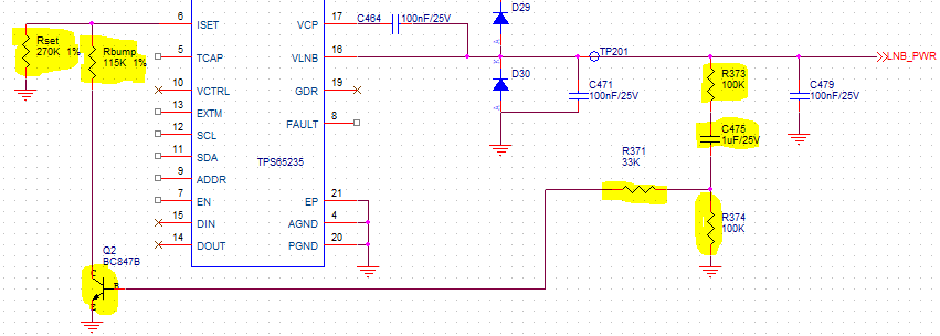
The problem is with correct selection of values of Rbump. Datasheet of TPS65235 states the typical relationship between Rset and output overcurrent threshold. The equation and chart given is accurate with measurement results up to 800-900mA. When comes to overcurrent limits above 1A, the equation is not valid anymore. I am afraid that the tolerances of overcurrent threshold also will be different that for 650mA (stated in datasheet table).


Could you give exact value of Rbump or design guides to meet requirement of (temporal) 1A output current including tolerances and Tj 0..125 deg.C?  

  • Hi Damian,

    It's really a good solution to have higher OC limit during start up.
    Rbump is only used at the startup and provide a 1A current limit right? So I don't think it needs to be very accurate.
    The RSET-ISET curve is actually a mathematical fitted curve. Any value set around 1A or a little higher should be good.

    Regards,
    Hao
  • Hi Hao
    The problem is, that the output current higher than 1.5 A is triggering the PSU overcurrent protection. This cause whole system power panic and shutdown, which is unaceptable. Limit 1.5A may be lower, depending on system load. That is why we need to be accurate, to meet NORDIG and to not trigger overcurrent. Could you help on what i requested?
    BR
    Damian

  • Hi Damian,

    OK, I see. I will go to check the information. Will update with you once I get something.

    Regards,
    Hao
  • Hi Damian,

    We have test items after the ICs fabricated to guarantee the resistor value lower than 1A, but the test is in room temperature. We don't have data in full temperature range.
    So, please set the Rbump at ~190k to have 1A current limit during soft start.

    Regards,
    Hao
  • Hi Hao,

    Thanks! That is what I expected.

    In beetweeen time I found another issue. For higher output currents the overcurrent circuit works unreliable. I found that this is due to my wrong layout - AGND pin where connected to slug and slug where connected to PGND. Noise from PGND where coupled to AGND. This caused unstable overcurrent protection. After cutting AGDN pin from slug, and connecting to analog decoupling plane, the issue disappear.

    I checked EVB reference layout. I checked recommended layout in dataheet, there is discrepancy between them.

    Please tell which AGND pin layout is correct? This is urgent. HW design release is tomorow.

    AGND to slug? (From datasheet)

    PGND to slug (From EVB)

    BR

    Damian

  • Hi Damian,

    I suppose the slug means the thermal under the IC.
    Actually, none of the two layout connect AGND and PGND to the thermal pad at the same time. That's the point.
    On the layout example on datasheet, AGND is connected to the thermal pad, but PGND is not connected to the thermal pad. On EVM, the situation is reversed.
    The basic idea is keep the sensitive AGND away from the noisy PGND. So, either of the layout is good. You may choose any one to follow.

    Regards,
    Hao
  • Hi Hao,
    I will follow EVB way to connect PGND to termal slug and AGND pin to signal plane.
    Many thanks for all your help!
    BR
    Damian