This thread has been locked.

If you have a related question, please click the "Ask a related question" button in the top right corner. The newly created question will be automatically linked to this question.

TPS61090: SW pins not working continously when attached microcontroller in ULP mode

Part Number: TPS61090

Hi

For my first question on this forum, I'd like to describe the following case:

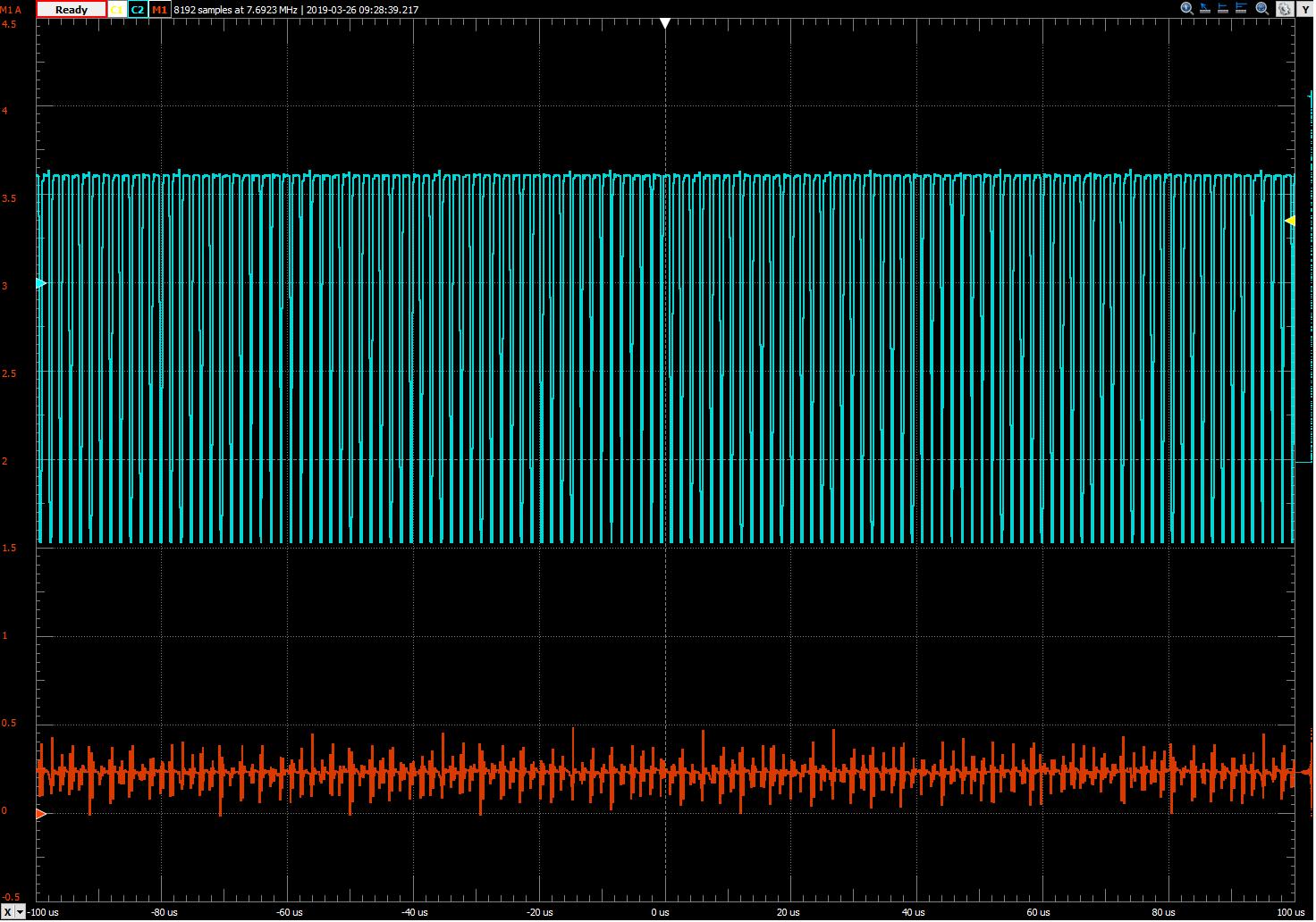
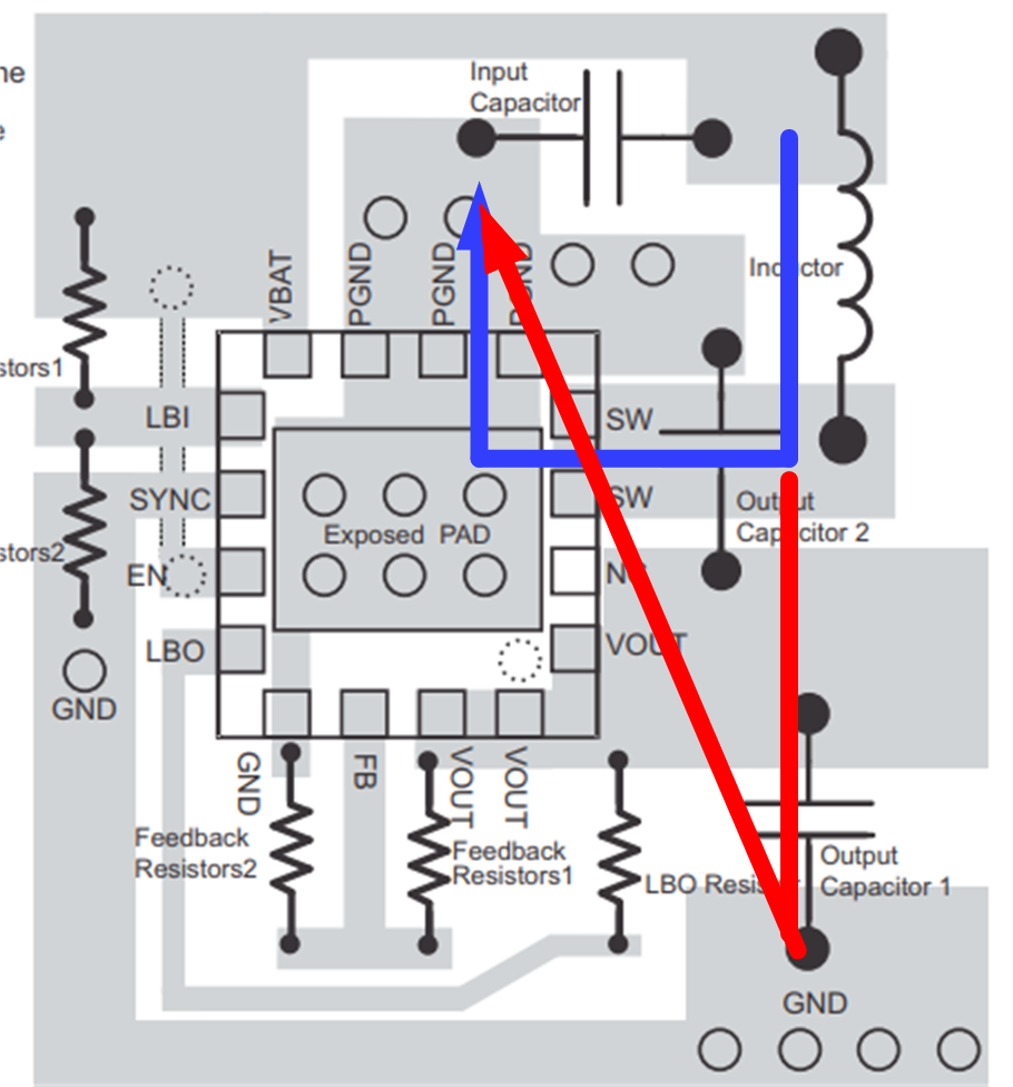
  • I have a TPS61090 with single cell battery input which provides 5.2 V to a microcontroller (NXP Kinetis K66) and an analog audio amplifier circuit (after a double LC filter, not on the schematic capture). In working mode, the circuit seems to work well and the SW pins switch at 600 kHz as they should.

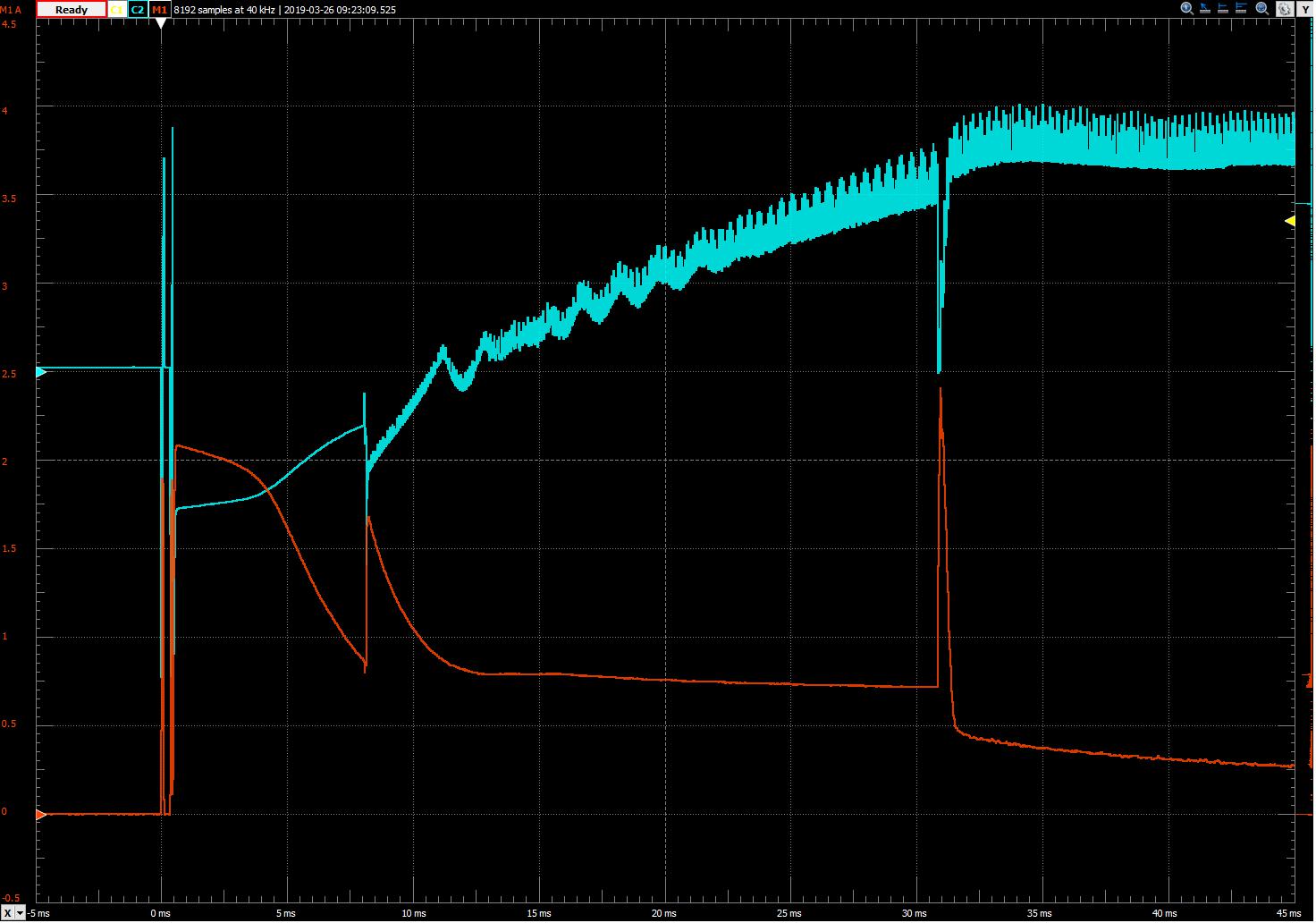
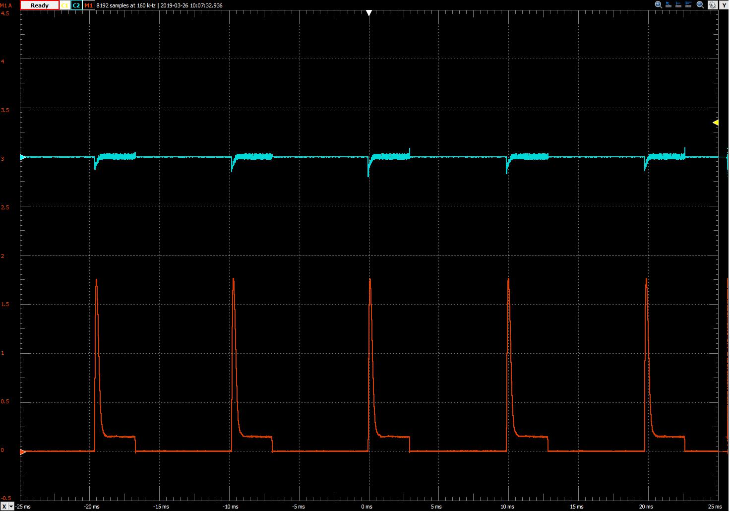
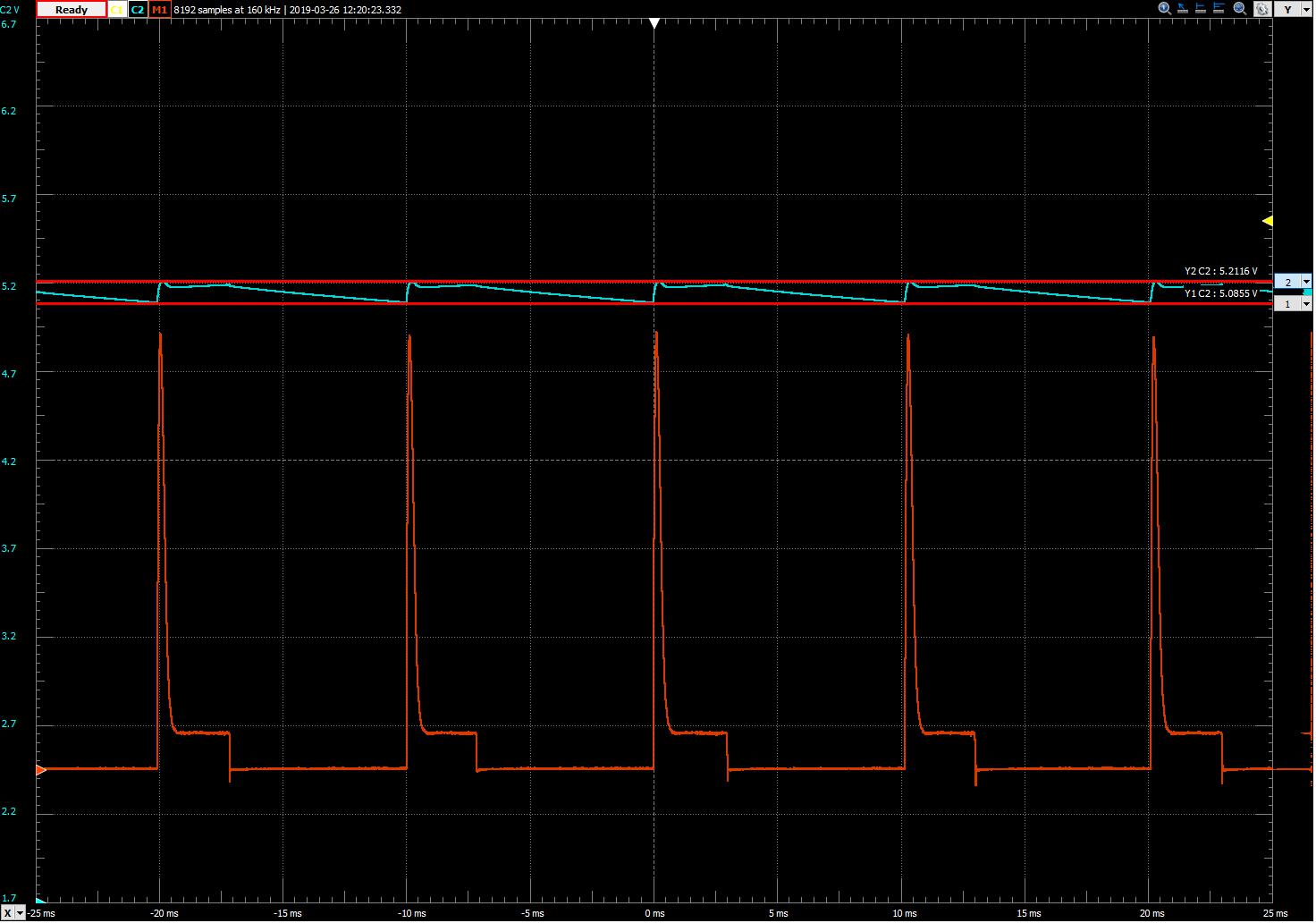
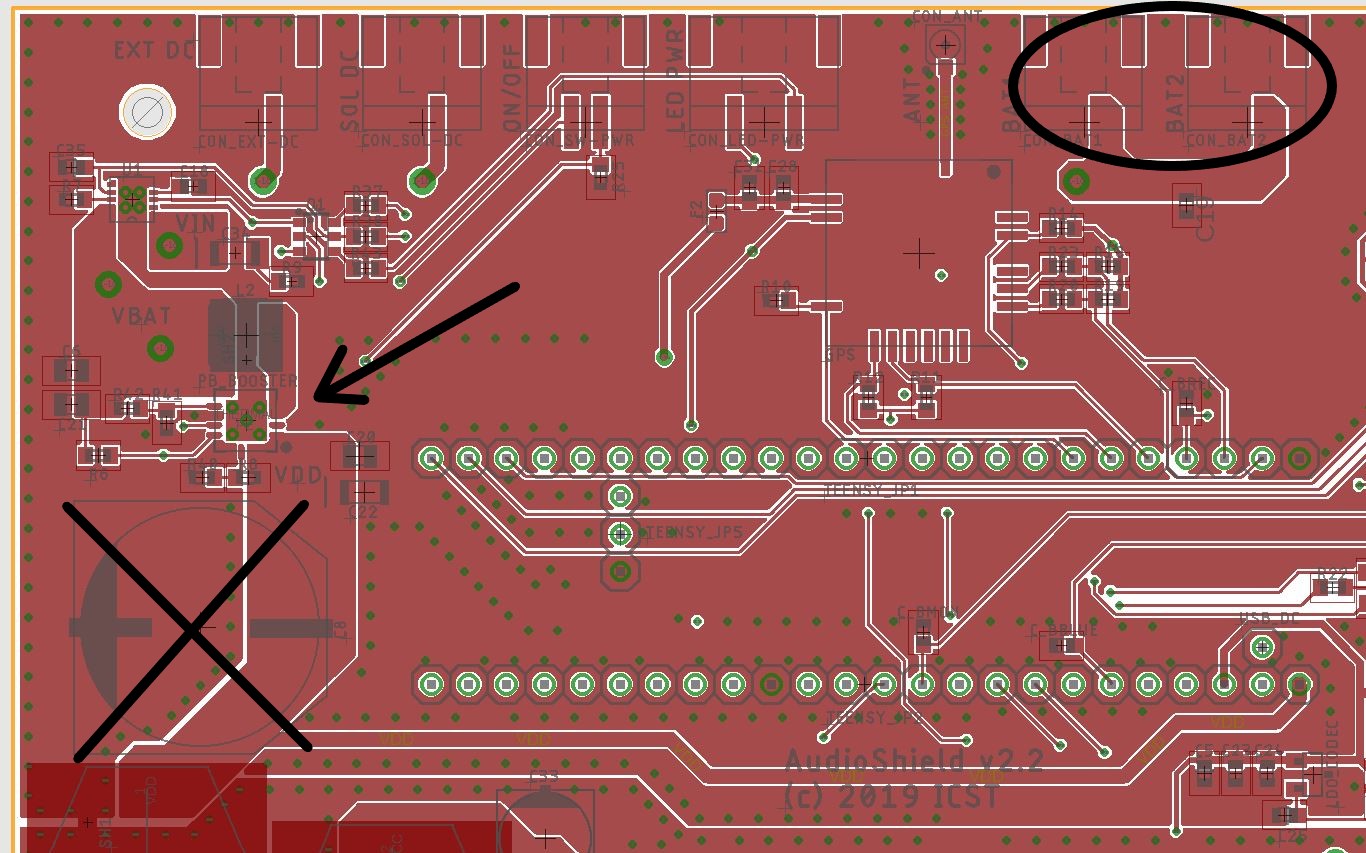
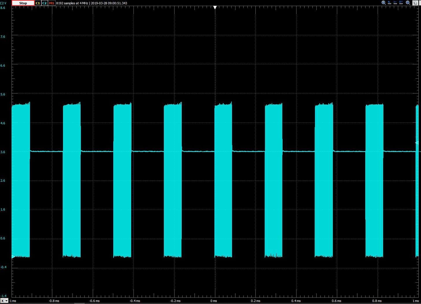
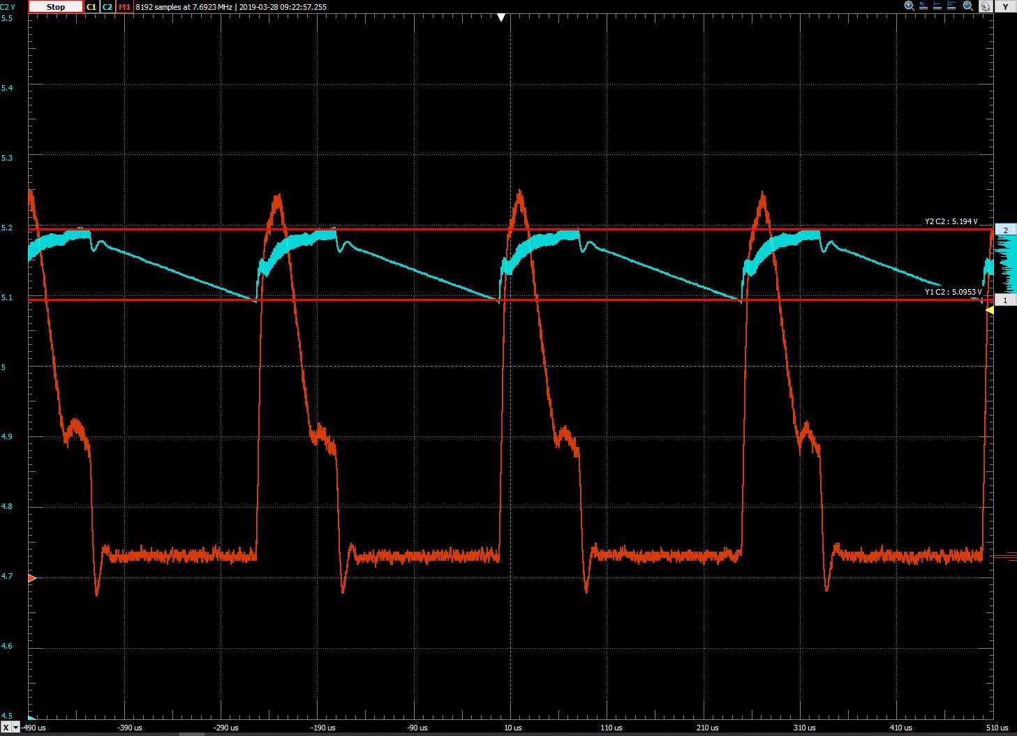
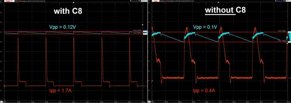
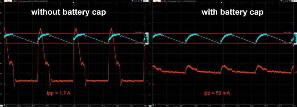
  • When the microcontroller is set to low-power mode (VLLSx), the SW pins alternate switching/stopping at about 100 Hz. And when the switching sequence starts, one notices an important voltage drop (up to 500 mV) in the battery, which corresponds to a ~1.5 A current peak... not really what I am looking for at low-power.

Do someone have an idea, why the behaviour changes with the power mode? Can that du to the 4700 uF capacitor (C8) that I put at Vout to smooth the output?

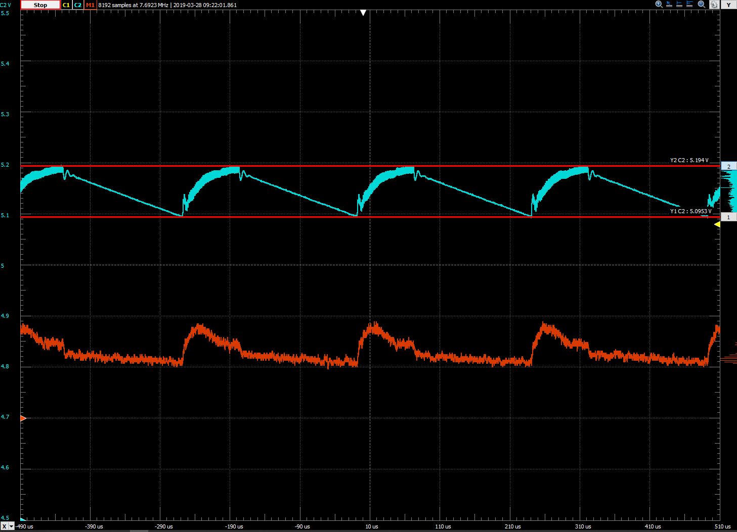
I can provide some layout documents and oscilloscope captures when I'm back to the office. But my mistake is perhaps so big, that someone can tell me straight away what to change...

Thanks in advance for any advice.

Best, Sébastien

  • Hi Schiesser,

    The device enters into PFM in light load condition, so SW pin swithes at very low frequency.
    It will help me a lot if you can share the key oscilloscope captures. When switching sequence starts, besides an voltage drop in the input, how about output voltage?
  • Hi

    Thanks for this advice that I somehow overread. Here you have some captures:

    First the measurement setup:

    Then the current peaks when I switch on the device (several module starting up after some initialization delays):

    Here the "normal" working mode (Fsw = 620 kHz, current = 200 mA):

    Finally the PFM mode @ 100 Hz (current peak = 1.7 A):

    Do I need some (more or replacement) cap to smooth these peaks?

    Best,

    Sébastien

  • ...here a capture of Vout (blue) and C1. I tried to put a big capacitor (4700 u) between the battery poles but without success.

  • Hi Sebastien,

    Thanks for sharing the waveforms.
    If the load doesn't need a very big load transient, the big cap is not necessary to solder. Such a big cap will cause big input current.
    Could you test it again without the big cap. And share the layout. Thanks.
  • Hi

    Which "big cap" do you mean? The one I attache at the battery poles or C8 shown right in the schematic of my first post?

    Thanks, Sébastien
  • Hi Sebastien,

    The output big cap C8.
  • Hi Zack

    First the layout. The booster circuit is top left where the arrow points. The circle shows the batteries connectors (2 single cells, but I made my test with one only). C8 at bottom left has been removed yet.

    Now some measurements. Without C8 the booster switches at 4 kHz and not 100 Hz anymore:

    Removing C8 doesn't change the amplitude of Vout transients (blue), but reduces those at Vbat thus the current peaks (red, Ipp = 0.57A):

    When I put a big cap (4700 uF) at the battery poles, the current peaks go back to Ipp = 90 mA):

    That my current state. Is there something in the layout that I could optimize?

    Best,

    Sébastien

  • Hi Sebastien,

    1. I have one doubt about your reply above: Removing C8 doesn't change the amplitude of Vout transients (blue), but reduces those at Vbat thus the current peaks (red, Ipp = 0.57A). Do you mean after removing C8 will reduce the input current peaks? But from your description then, after putting a big cap, the input current peaks go back to 90mA?

    2. The device works at PFM mode at load load currents to maintain a high efficiency. It will switch for some time to regulate the output voltage to reach upper limit, then stops switching. So you can see when output voltage reaches to 5.194V, output voltage drops to lower limit 5.095V with no switching. That's the reason the vout ripple is same no matter whether you put C8 or not. However, put such a big cap will need more energy from input to charge it to upper limit. So I recommend you not put such a big cap.

    3. higher input current will cause input voltage drop. So a bigger cap is recommended to add close to the IC. It will supply energy to the output and input voltage could sustain at a stable level.
  • Sorry I think I haven't been really clear...

    1. I removed C8 (4700 uF) at Vout and let both other capacitors C20 and C22. This didn't change the peak-to-peak amplitude of Vout as you can observe on the capture (left: with C8, right: without C8). But the current flowing from the battery is reduced to 1/4.

    Then, after having removed C8, I added another 4700 uF cap at the battery poles, like your application note SLVA236A (p.5-6) recommend. This reduced the current peaks again to 50 mA (wrote 90 mA but forgot to remove the current offset due to the small measurement resistance).

    2. & 3. are (I think) clear for me. The only topic I am not sure about is perhaps parts placement or layout...

    Regards,

    Sébastien

  • Hi Sebastien,

    Thanks for explaining the graphs again. It's really hard to see clearly the vertical scale of previous graphs but now everything is clear.

    So in summary:

    1. Remove C8 and add battery cap.

    2. Layout could be optimized. Right now it's not good.

    Below is the recommended layout in the datasheet. Input capacitor, output capacitor, and the inductor should be placed as close as possible to the IC. Reduce the current trace length.

    The C6, C21 is quite far away from IC, and please add some ground vias close to negative pad of C6, C21. Place C6,C21, L2, C20, C22 like the above picture. And place several ground vias next to negative pad of C20, C22.