This thread has been locked.

If you have a related question, please click the "Ask a related question" button in the top right corner. The newly created question will be automatically linked to this question.

UCC20520: PWM signal distorted at the IGBT's gate.

Part Number: UCC20520

Hello everyone, I appreciate your help me to figure out what is my problem,I just started to use the driver UCC20520 and i don't have experience using this devices.

Thank you in advance.

I´m using this driver to control a half bridge inverter where is connected a single-phase motor, which nominal current consumption is about 20Amps-Peak (13Arms) and at the starting up to 35A-peak, 179 VDC-link voltage. Is supposed that my IGBTs can drive that current but i´ve blowing it up.

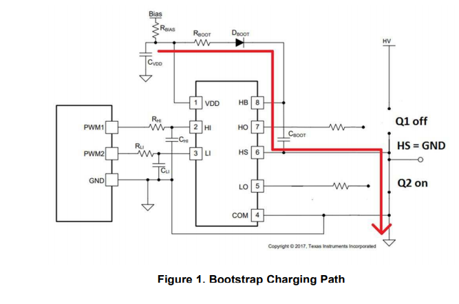
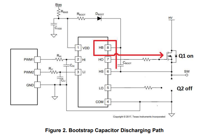
In the next diagram show how the circuit was connected and the values that were use. DIS pin was grounded without resistance and diode and resistance inside dotted lines were not used, Rgs = 10K, Ron = 10, Cboot = 1uF(metallic polymer), Rboot = 10, Rdt = 75K. the bootstap diode is an 1N4007.

Is it necessary to use the resistance and diode to discharge the gate?

The bootstrap diode, what is it for?

How the Ron affects the behaviour of the leg?

This is how i´ve connected the driver, DIS pin is grounded and the resistor and diode in the dotted lines were no connected.

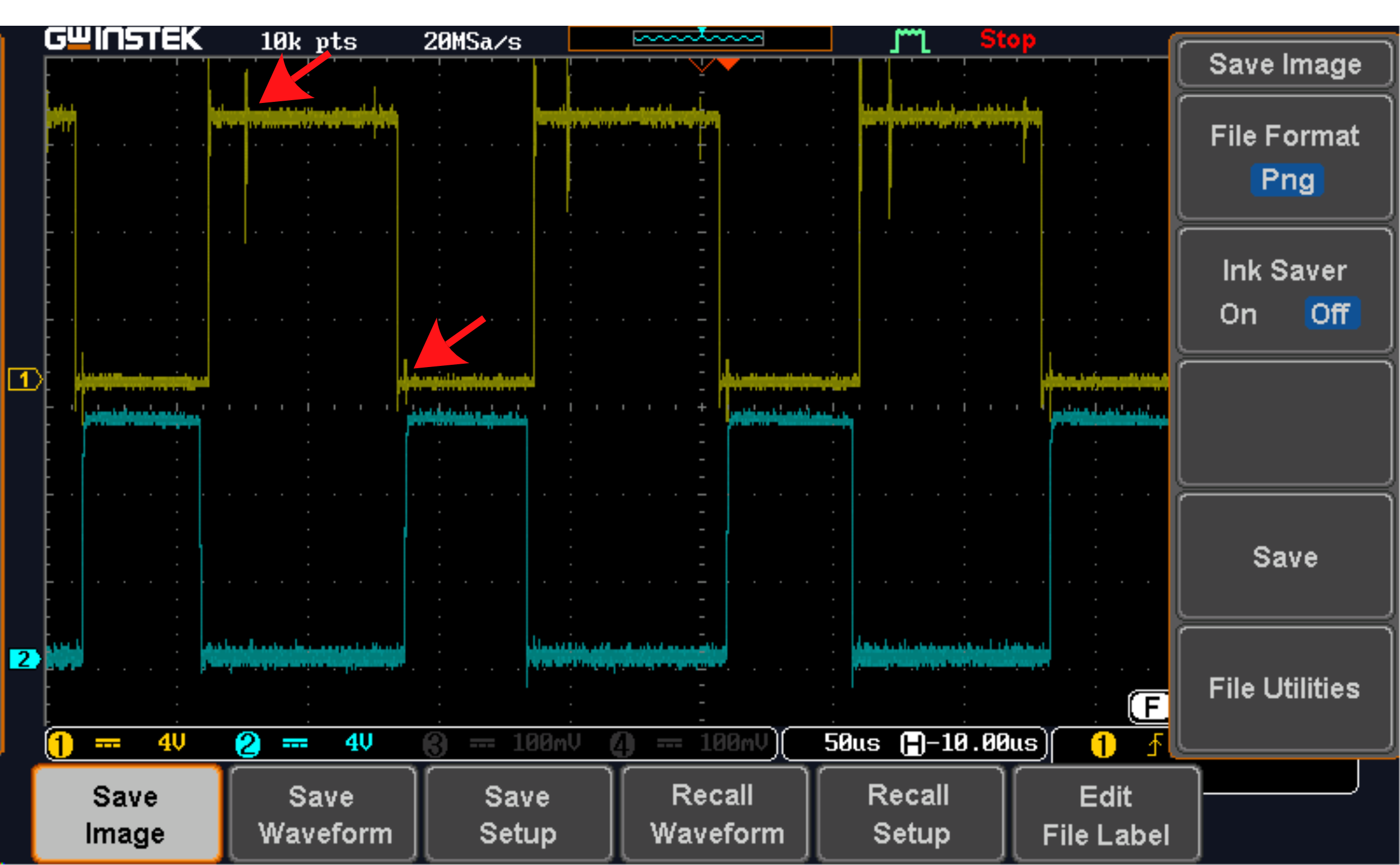
The signals that I got are the next ones:

  • in the first screen are showed the voltages at the gates, the blue one is the high side and de green one is the yellow.
  • The second is the voltage between phases,

Is it normal to have those voltage spikes?

And related with the code to generate the SPWM signals, how the minimul pulse width affects the UCC driver?

because i noted that if this is to small it can distorted the pwm signals.

  • Hi Edd,

    Thanks for interest in our device, my name is Mamadou Diallo, I will help address your question.

    1. "Is it necessary to use the resistance and diode to discharge the gate?"

    The anti-parallel turn-off resistor and diode are not required but highly recommended to enhance the turn-off speed of the design. These will help provide a low impedance path for the discharge currents to speed up turning off the FET while blocking the turn-on path that you control using Ron to limit the dv/dt at the gate and prevent overshoot. Section 3.4.1 of the document below discusses this in further detail.

    2. "The bootstrap diode, what is it for?"

    This diode first role is to provide path from the supply cap Cvcc to charge the bootstrap capacitor during the off transitions of the high-side FET as shown on the diagram below:

    During the high side on transitions, the boot diode blocks the charge from boot cap and protect the bias supply as shown below.

    You can further on this on the attached documents: 

    Looking at your waveforms however, there is quite bit of ringing on the yellow waveform. Can you confirm whether that is the high-side gate or the low-side.

    The blue waveform looks reasonable on the other hand.

    Also please zoom-in on one to see how high the overshoot reach because if you exceed the recommended operating conditions, the driver might misbehave which might explain the damage you described.

    This overshoot at the gate may be caused by many factors including effects of parasitic inductance which occurs when the FETs are connected to the driver using long PCB traces. Is your high-side gate captured using a differential probe between high-side gate and switch node (SW)?

    Also as sanity check, how much is bias capacitor? Cvcc? this capacitor needs to size large enough to provide sufficient charge to the bootstrap capacitor. We typically recommend Cvcc to be 10x larger than Cboot to deliver the required charge on the boot cap.

    Your values for  Rgs = 10K, Ron = 10, Rboot = 10, Rdt = 75K seem reasonable but how much gate charge are you expecting from the FETs? Depending on that you can review your boot cap value (using attached app note) to ensure it also sized accordingly.

    I am curious to see what the switch node to GND waveform looks like.

    Regards,

    -Mamadou

  • Hi Edd,

    I have not heard from you. I must assume that you have resolved the issue, I am therefore marking this thread as closed.

    If so, feel free to share how you resolved the problem for other e2e users to benefit from.

    However if you're still having difficulties with our driver, please let us know to address the issue.

    Regards,

    -Mamadou