This thread has been locked.

If you have a related question, please click the "Ask a related question" button in the top right corner. The newly created question will be automatically linked to this question.

TLV62568: Minimum Load Current

Part Number: TLV62568

Hi,

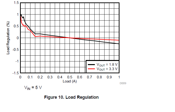
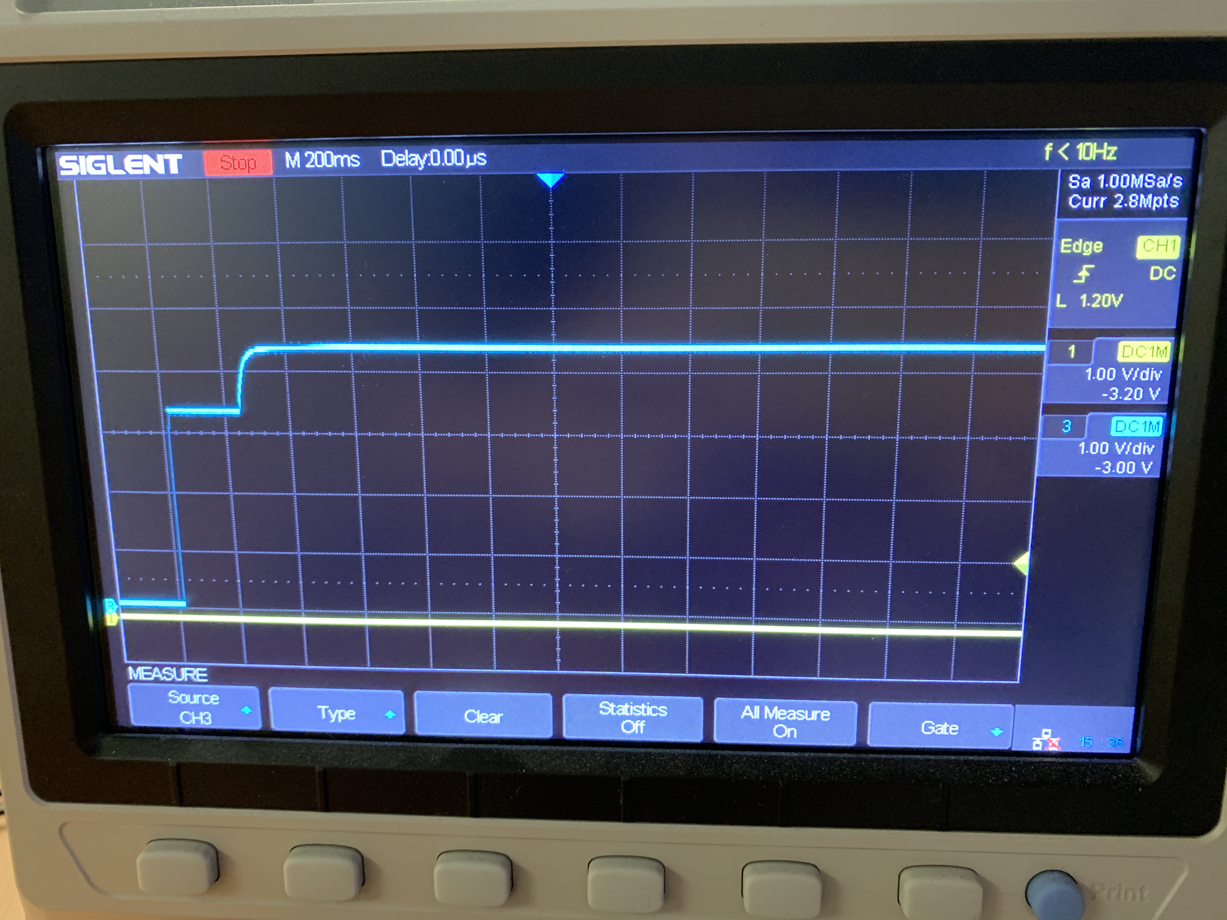
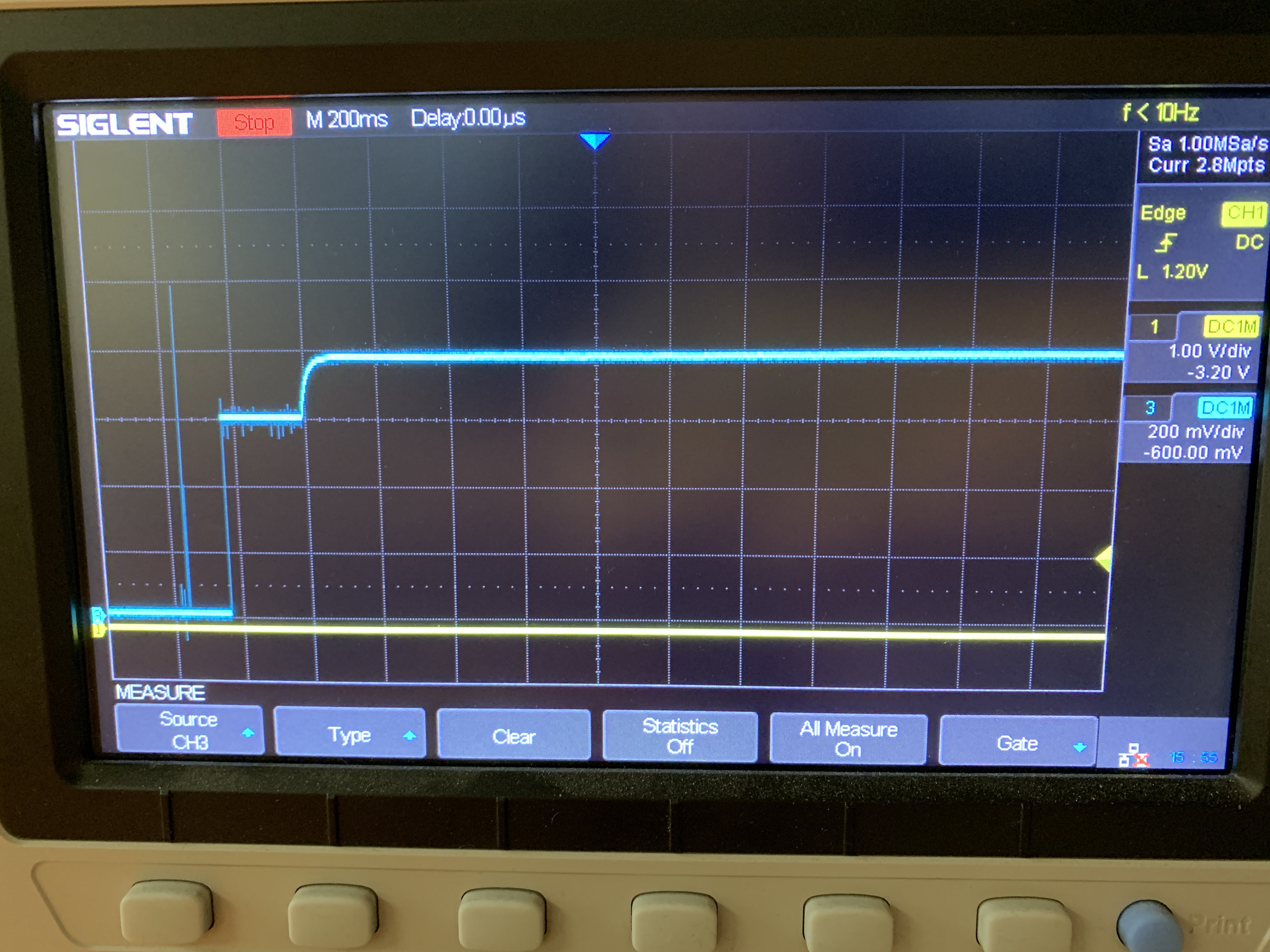
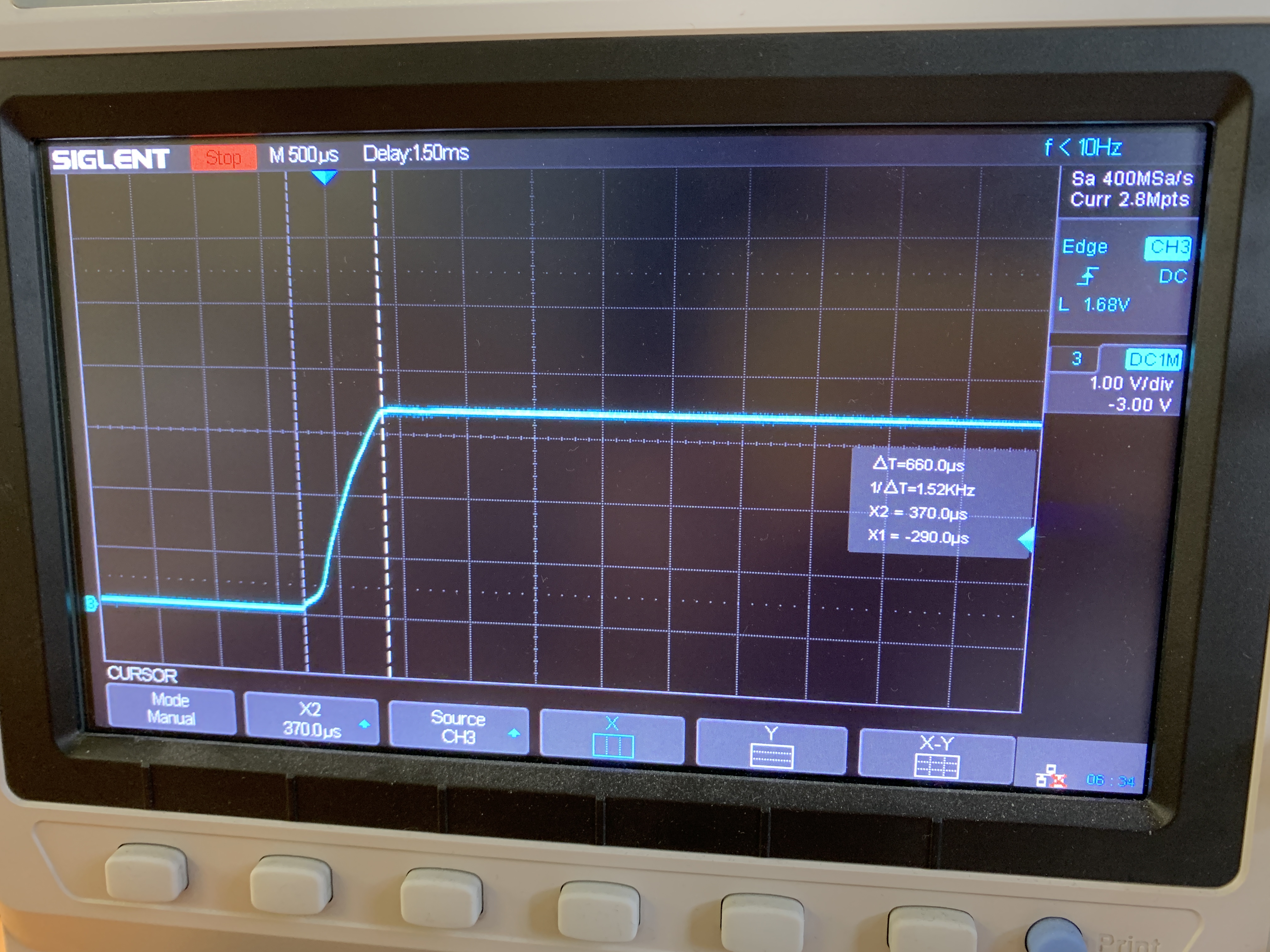
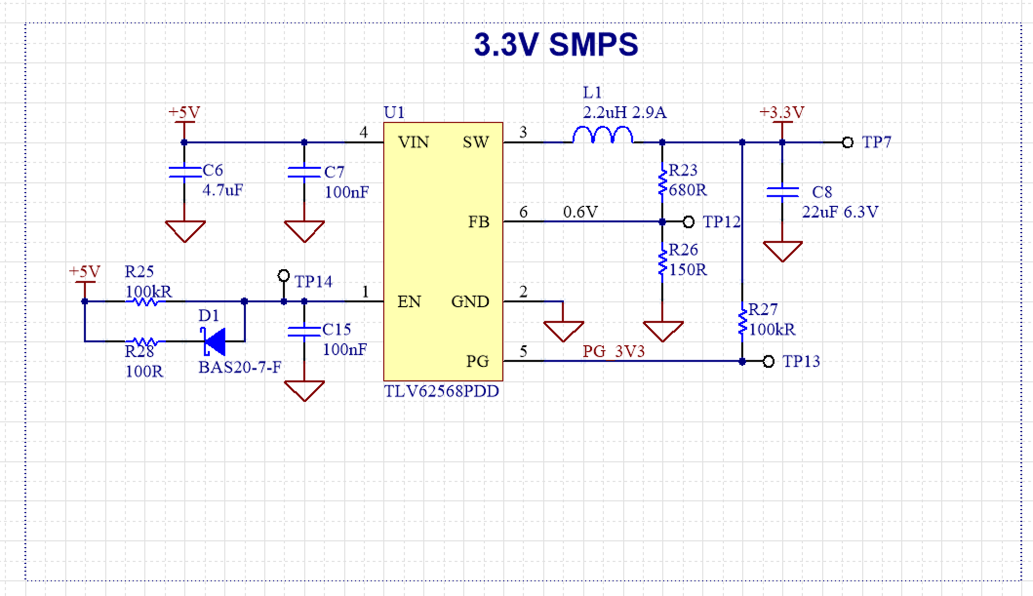
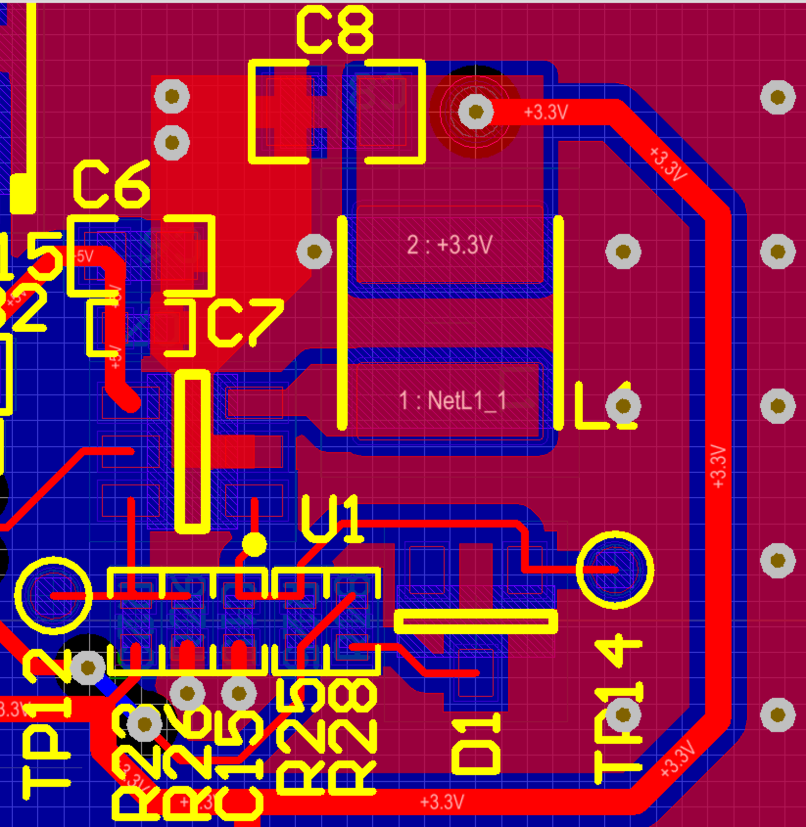
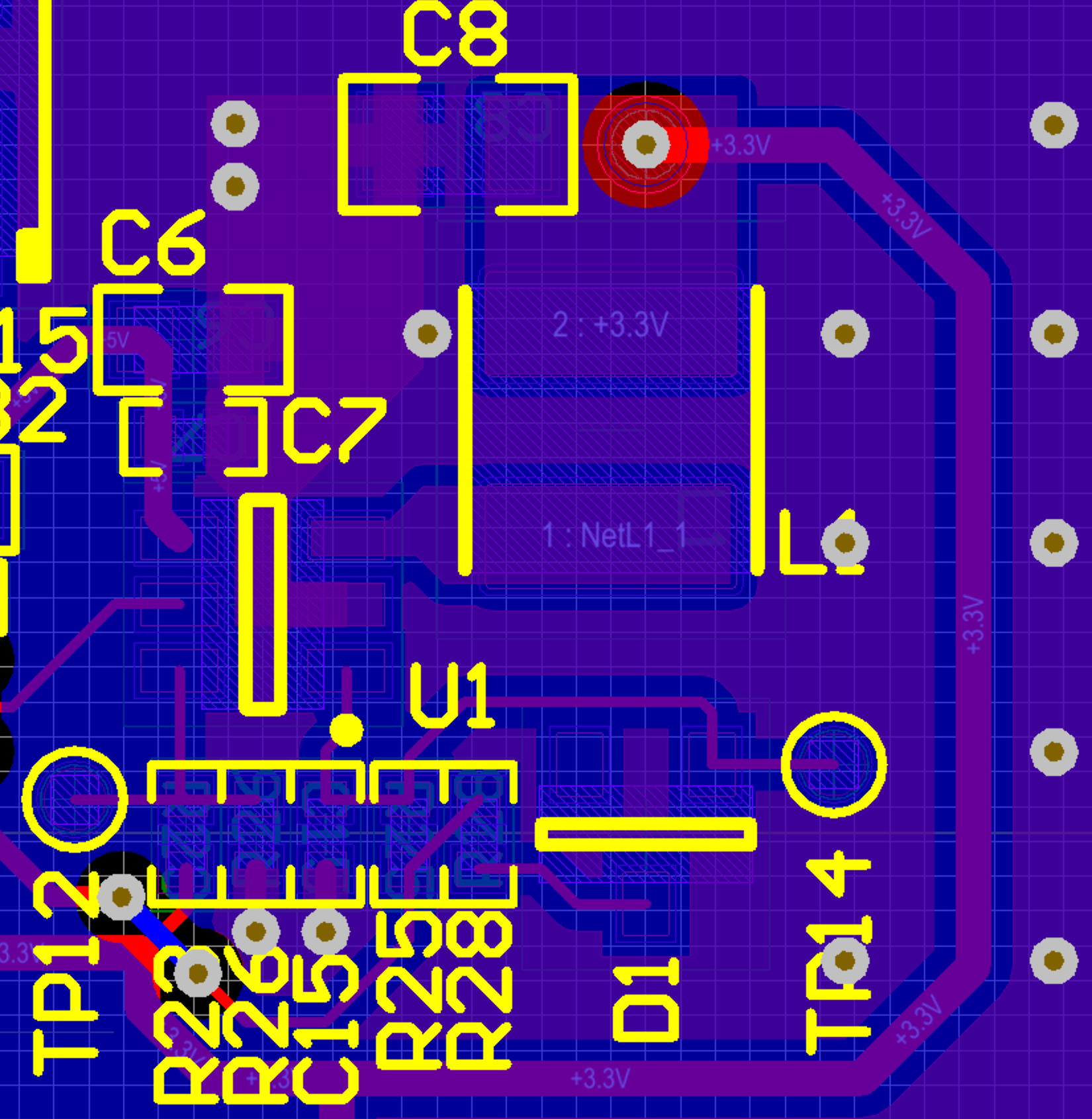
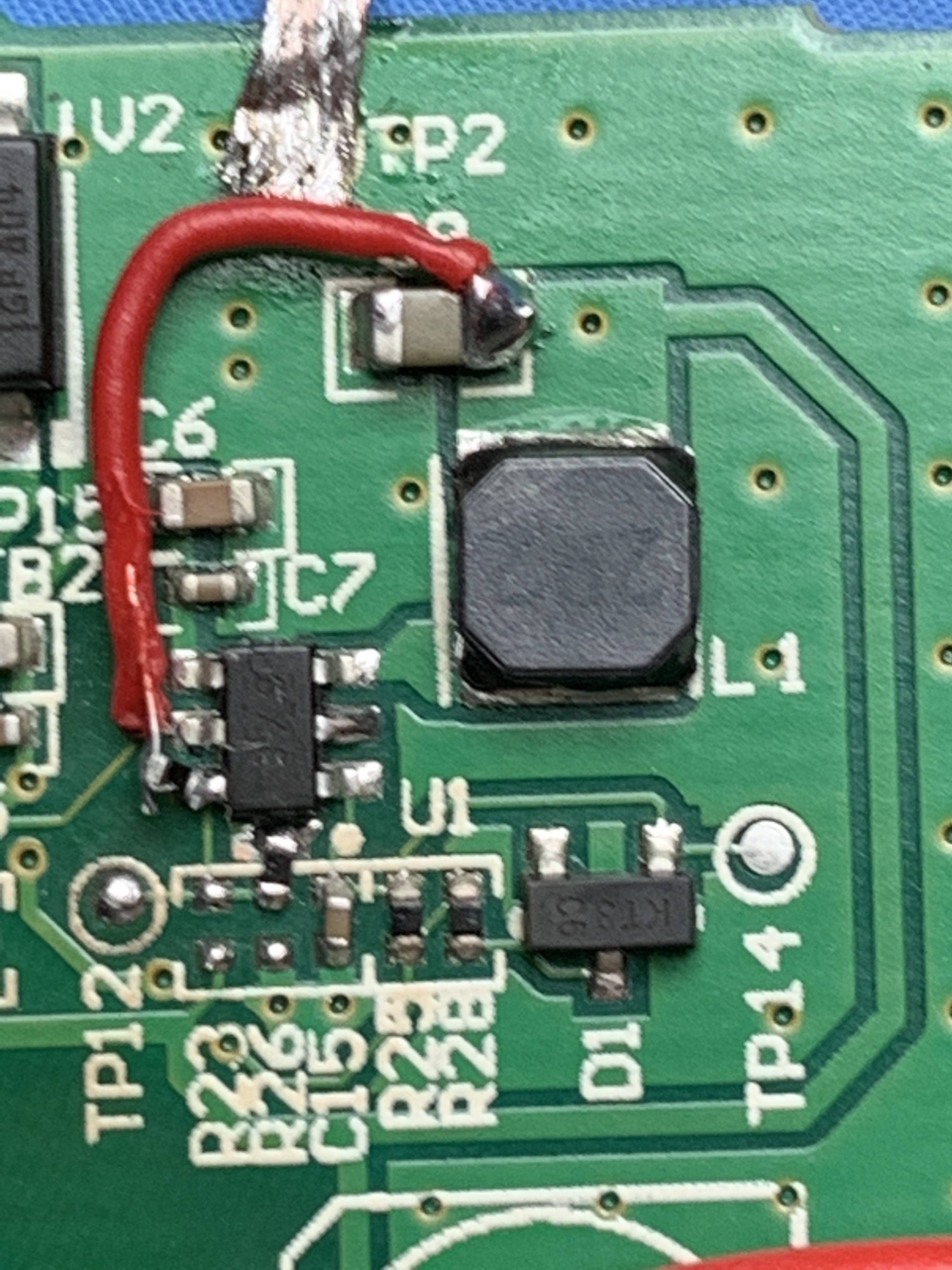
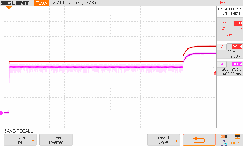
We have used the TLV62568PDD in our design to regulate a 3.3V supply from 5V nominal input.  The Power supply was designed using the Webench Power Designer.  We have designed for 400mA Imax, but typically we are only running at ~50mA.  We have noticed a strange issue on startup and MCU restart conditions where the load on the Power supply is drastically reduced to 550uA.  In this scenario, the output of the TLV62568 increases from 3.3V up to ~3.7V (12% increase), and the Feedback voltage increases from 600mV to 664mV. 

I guess the first question is: Is this normal behaviour for this IC?  I have not seen anything in the datasheet that suggests that this is expected behaviour.  Perhaps someone that is familiar with this IC is able to confirm whether they have experienced this as well?

In the meantime, our workaround solution is to apply a resistive load to ensure the minimum output current does not drop below 5mA.  This is hardly an ideal solution, I hope that someone in this forum is able to resolve this issue.

Thanks in advance.

  • Hi Stephen,

    This is not a normal behavior. As per datasheet, load regulation at no load at 3.3V output is ~1% (see graph below). In addition, VFB regulation is within 0.588V to 0.612V only.

    Does the output voltage stay at 3.7V or it drops to 3.3V after sometime with Io < 500uA? Can you give output voltage waveform at start-up? Please provide the schematic diagram, PCB layout and BOM related to the IC.

    Thank you.

    Best regards,

    Excel

  • Thank you for taking the time to look at my issue.

    I have done further testing on our hardware today and have further observations in addition to the materials that you have requested.

    Critically, I removed all other components from the PCBA so that only the Power supply is operational with no load.  In this mode, the power supply is operating as expected with load regulation deviation as per the image you sent through. 

    We have managed to link the behaviour to one load, that being a CC3220 module from a third party supplier.  The interesting thing is that the behaviour persists even when the chip is held in reset.

    When we disconnect the CC3220 from the power supply the issue goes away.

    Upon further testing today, I realise the power supply can reach nearly 4.5V in certain scenarios.

    The below image shows the output supply from the TLV62568 when the CC3220 is held in reset on powerup.

    Interestingly, the power supply is stable at 3.3V for approximately 200ms before it increases and tends towards 4.5V.  To answer your question, the Power supply does not recover unless I increase the load current.

    Image showing the 3.3V TLV62568 output on startup with CC3220 held in reset and output current <1mA

    Image showing the feedback pin of TLV62568 output on startup with CC3220 held in reset and output current <1mA

    Enhancing the startup for 0V to 3.3V region:

    The Schematic is as follows:

    The PCB is 2 layers and is as follows:

    Here is the BOM for the SMPS.

    Comment Description Designator Mftr. Part # Mftr.
    2.2uH 2.9A IND 2.2uH 20% 2.9A 3AIsat 37mR L1 ASPI-0418FS-2R2M-T3 Abracon LLC
    4.7uF CAP 4.7uF X5R 10% 10V 0603 C6 CL10A475KP8NNNC Samsung
    22uF 6.3V CAP 22uF 6.3V 10% X5R 0805 C8 CL21A226KQCLRNC Samsung
    100kR RES 100kR 1% 100ppm 1/16W 0402 R25, R26, R27 RC0402FR-07100KL Yageo
    100nF CAP 100nF X7R 10% 16V 0402 C7, C15 GRM155R71C104KA88J Murata
    100R RES 100R 1% 100ppm 1/16W 0402 R28 RC0402FR-07100RL Yageo
    BAS20-7-F DIODE BAS20-7-F 1.25V @200mA, 200mA, SOT23 D1 BAS20-7-F Diodes
    TLV62568PDD REG Buck, Vin2.5-5.5V, Vout 0.6-5.5V, Iout 1A SOT23-6 U1 TLV62568PDDCT TI
    453kR RES 453kR 1% 100ppm 1/16W 0402 R23 RC0402FR-07453KL Yageo

  • Hi Steven,

    Thanks for the info.

    The resistor divider going to FB pin should be connected as close as possible to the output cap (C8). However, there is a long loop from the output cap going to R23. If my suspicion is correct, this same trace goes to CC3220 which makes it susceptible to noise that can disturb the voltage regulation of the FB pin as well as Vout.

    Can you try to disconnect the pin of R23 which is connected to 3.3V and then use a short jumper wire to connect it to C8? I hope this bypass the noise on the FB resistor divider.

    In addition, I noticed in your schematic diagram that the resistor divider (R23 & R26) values going to FB pin is quite low compared to the BOM list. What are the correct values for R23 & R26? If it is 680R and 150R, can you change it to 100K and 435K similar to the BOM list?


    Best regards,
    Excel
  • Hi Excel,

    Thank you for your comments and suggestions.

    Regarding the discrepancy between BOM and Schematic, please note the resistors are currently as per the BOM. I updated the schematic to increase the idle load on the Power supply and forgot to screenshot prior to making the changes.

    I have done as you suggested and moved R23 so that I could run a jumper wire directly between this FB resistor and C8.  Unfortunately, the output waveform still looks the same.

    I have also tried turning R26 around so that it connects to GND pin 2 of TLV62568 on the Top layer copper, again no difference was noted.

    Here is a photo of the circuit with the 2 modifications.

  • Hi Steven,

    Can you provide the following waveforms?
    1. Vout and VFB (50ms/div)
    2. Vout and SW node (a. when Vout = 3.3V; b. when Vout = 3.7V). Please measure the frequency of SW node each time.

    Is this consistent to other unit? Did you try to replace the device? Is the behavior still the same?
    I just wanted to ensure that the part is not yet damaged.

    Thank you.


    Best regards,
    Excel

  • Hi Excel,

    The problem is widespread and is not limited to a single device.  I replaced the TLV62568 with a brand new one (from a Digikey packet) this morning and it immediately did the same thing.  The Part marking ix 9X9 which you may have already deciphered from yesterday's photo.

    Here are the waveforms that you requested.

    1: Vout and FB at 50ms and 20ms

    2: SW node switching during at 3.3V

    The Frequency of switching varies considerably as you can see from the below picture (presumably in Power Save Mode)

    2b) SW node, there is no switching when Vout rises above 3.3V

    2c) SW node, at the time the voltage rises from 3.3V

    Thanks,

    Stephen

  • Hi Steven,

    I highly appreciate your effort for providing the necessary data.

    I'm pretty sure the +3.3V output node is injected by a higher voltage from an external source which possibly came from CC3220 circuit. Because FB pin will not allow to exceed its regulation voltage unless it came from an external supply on the output.

    As shown in the waveform, the SW node stops switching after ~220ms because the FB is >0.6V which means that the buck converter circuit is not delivering current to +3.3V for it to sustain its voltage level or even higher.

    To verify my theory, don't apply Vin on TLV62568. Apply the supply on CC3220 then measure the voltage on +3.3V. I will not be surprise that the output voltage level is same (>3.3V) as what you are seeing now. If this is true then the issue is not due to TLV62568 but from an external source.

    Looking forward for your feedback.


    Best regards,
    Excel
  • Hi Excel,

    You are correct.

    It turns out the factory has loaded a Push/Pull Voltage detector on our PCB which was injecting 5V into our circuit.  I'm annoyed I didn't pick up on this sooner but very much appreciate your assistance.

    Many thanks,

    Stephen