This thread has been locked.

If you have a related question, please click the "Ask a related question" button in the top right corner. The newly created question will be automatically linked to this question.

TPS53513: Negative currents during Load Transient

Part Number: TPS53513

Hi,

We are using TPS53513, specifications are listed at the end.

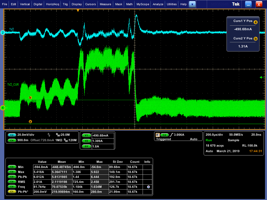
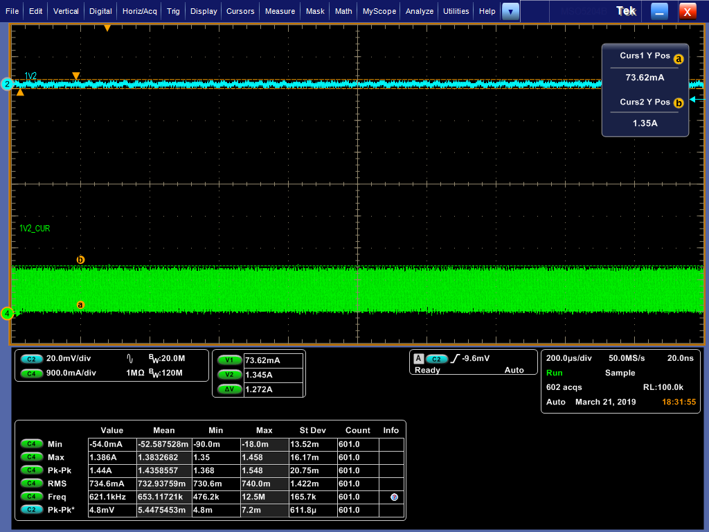
During Our testing we are seeing maximum negative current of around -1A, But as per datasheet,when we running in auto-skip mode, the negative currents are not possible(i.e Lower MOSFET willl be OFF as negative current is sensed).


After probing more, what we understood is most negative current is coming after current transient during settling. Captures are attached for reference.

Below are the questions:

1.Whether negative currents are allowed?

2. If negative currents are allowed, what will be the impact to the regulator , in addition to unnecessary power loss in regulator

3. How can i reduce the negative currents - Inductance is increased to 1uH, we are seeing improvement in negative currents in steady state case, but during transient case still we are seeing 600mA negative current.


Below are the specifications

Input :

VDD : 5V (4.5V to 5.5V)

Vin : 2.5V to 5.5V

Output:

Vout 1.2V,10%

Iout max = 6A

Circuit is as follows:

VIn Input capacitors : 5x22uF + 2.2nF

VDD input capacitor : 1x2uF

MODE pin - connected to GND with 0 Ohms resister.

RF pin : Resister divider from VREG using 249K and 105K (down resister)

TRIP pin : 38.3K to GND.

FB pin: REsister divider from Output voltage using 2 numbers of 10K resisters.

Inductor : 0.56uH

Output capacitors : 5x100uF+1x22uF+2x1uF

Snubber is in place.

  • Malli,

    Can you zoom in and show both the SW node and the negative current limit? Please show 3 to 4 switching cycles.
  • Hi,

    i have tested few scenarios.

    1. Tested with higher inductor values - 1 uH,1.5 uH - Peak -Peak Inductor ripple current is less,  little improvement in negative currents - but not solved the problem.

    2. Added a feed-through capacitor across upper FB resister , responses noted with different values of Feed through capacitor - 

    checked with feedforward capactors ranging from 33pF to 2.2nF.

    Best response is with : -1A current is reduced to close to -0.4A with 1000nf feedthrough capacitor + 1uH inuctor.

    Few of the switch node waveforms are attached below.

    This is for L=1uH & Cfeed = 470pF

  • Malli,

    That very much looks like FCCM operation. Are you sure you do not have MODE pulled up to VREG or PGOOD?
  • Currently MODE pin(21) pulled to GND using 0 Ohms resister. I have checked with DMM also. MODE pin is 0 Volts.

    Below is one more capture, I can see during transient ON time is kept constant and OFF time got varied.

  • Malli,

    How many boards exhibit this behavior? Clearly it is operating in FCCM mode. The SW node waveform has a distinct characteristic in DCM, which I do not see. If this is only one device, possibly it is damaged.
  • Malli,

    I have tested an EVM in the lab.  CH 1 = SW node, CH 4 = inductor current. Below waveform shows 250 mA load with MODE connected to GND to select SKIP mode.  You can clearly see the characteristic DCM waveform of SW when the inductor current falls to 0.

    Next see MODE pulled up to VREG to select FCCM.  Iout is still 250 mA.  Classic FCCM waveforms like yours are shown, with inductor current going negative.

    Conclusion: You are operating in FCCM mode, not SKIP mode.

  • Hi John,

    Thanks for the update. I am in another task for few days. That's why couldn't able to respond back.

    I need to confirm whether there is a problem related to MODE pin settings in current design or not?

    But our default setting for MODE pin is AUTO-SKIP mode. 

    current distribution in our captures in different. In EVM measurements for every cycle inductor current becoming "0" and stays that level for some time and then ON time starts.

    But in our case, we see 4-5 cycles before current stays stable "0"A level.

    Anyway, i will check and update..

  • Malli,

    The green trace is SW node (inductor current) and it is offset by 1 A, correct? It would be easier to get an accurate measurement if you set the offset to 0 A. It looks like you are right on the edge of DCM operation. If you decrease the load more you should start to see the characteristic DCM current and voltage waveforms as shown in my previous post.
  • Malli,

    I will close this thread for now. You can re-open it any time by responding to it.
  • Hi John,

    Now i am doing this testing.

    Things i confirmed is TPS53513 is configured for Auto-skip mode.

    With Inductance increased to 1.2uH and with feedforward capacitor of 1.5nF - I can see most negative current is reduced to -160mA.

    It was tested in multiple boards, I am not seeing whatever standard Auto-skip mode characteristics on Switch node waveform(as shown in EVB). 

    Can you confirm whether in Auto-Skip mode, is there any possibility that negative current (flowing inwards to Synchronous mosfet) flow?

    What is the impact of this negative current on design, power dissipation or reliability/life time of the chip etc.

    I will add few captures to this tomorrow.

  • Malli,

    I am not sure what you are doing wrong.  In auto skip mode, the SW voltage and current are what I showed previously.  I have never seen it operate any other way.  I'll check your wave forms tomorrow.

  • Malli,

    Also can you post your actual schematic and PCB layout? I can't think of what layout issue could cause your problem, but it won't hurt to check it.
  • Hi John,

    Sorry for the delay.

    We can't share the design over the forum. Can i get Local FAE for TI support in Bengaluru(Bangalore), INDIA region.

    I have asked another question, according to FCCM captures, we see negative currents occurring.

    What will be the impact of negative currents on regulator endurance/reliability.

  • malli,

    I suppose can contact your local sales office. I cannot really comment about how support works in India.
    TPS53513 is designed to operate in FCCM mode. In FCCM, there will be negative switch current when Iout is less than ILp-p/2. There is no risk for it. There is a negative current limit, see the datasheet. You should design so that ILp-p/2 is les than that so you do not hit the current limit in no load condition.