This thread has been locked.

If you have a related question, please click the "Ask a related question" button in the top right corner. The newly created question will be automatically linked to this question.

BQ76200: Charge Pump not working on power-up

Part Number: BQ76200
Other Parts Discussed in Thread: CSD19536KTT,

The charge pump operation is intermittent. This is related to power-up (connecting battery or bench supply to the BAT side of the circuit). Once connected and functional it appears to run with no problems. The intermittent refers to the initial connection. If I cycle power on the BAT a few time and get it to come up, it works and continues working.

Cap at VDDCP is 2.2uF/25V to provide sufficient capacity for 8ea CSD19536KTT FET's. Filter is 100ohm/.01uF. 75V Zener to protect part.

Battery operates 45-60V, testing at ~52V as described below.

I reproduce the problem as follows:

Connect BAT (with all BQ76200 signals low). Pull CPEN high, monitor VDDCP, leave all other control signals low.

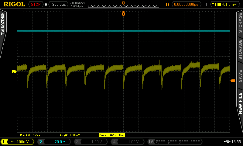
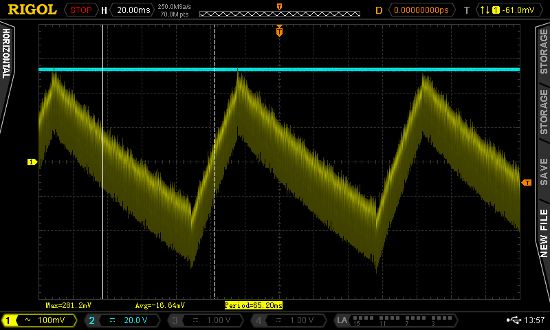
- Sometimes the charge pump generates ~1V (so VBAT + 1V). In this mode it is a steady 1V, no charge pump waveform. Enabling CHG or DCHG makes no difference.

- Sometimes the charge pump generates 10V (so VBAT + 10V). In this mode the charge pump sawtooth waveform rides on top of the 10V. Enabling CHG or DCHG works as expected (FET gates rise ~10V above VBAT).BQ76200 Circuit.docx

I'm attaching a word doc with the schematic snippets (hope it shows).

  • As an update, I have been able to reproduce the issue without disconnecting power.
    With all control inputs low, if I bring CPEN low and back high the charge pump does not turn back on reliably.
  • Hi Gerry,
    The schematic looks reasonable, in the description the charge pump would be trying to start without load. If it can't start it either has a supply problem, internal failure, or excessive load. It is not obvious that any of those would be intermittent.
    You might check for contamination around the IC pins or C7. When the charge pump is loaded it will deliver fixed voltage, if it can't reach full voltage it won't cycle as you see with the 10V output case. You might also check the measuring instrument to be sure it provides a consistent load, the charge pump will typically drive a few 10M probes to GND but may not drive less. You might also try to replace either the IC or C7. I have heard of capacitors exhibiting time-variant limiting behavior.
  • I have several boards and all have the same issue (3 so far anyway) so it's unlikely a bad component. The board is clean, no visible contamination. Is the X7R capacitor a good choice for this application?

    At the moment CPEN has no affect unless it keep it pulled up and cycle power, then the charge-pump comes up.

    One thing I see is ~150mV @ 250uS of noise on the power. Probably from the 5Vcc switcher on-board. I'm including a couple images of VDCCP (it looks the same with CPEN low or when CPEN is high and it doesn't come up with the exception of being ~1V higher). When it comes up it is obviously different with the sawtooth waveform riding at ~10V above VBAT. Is this level of noise an issue?

  • Ran a couple more tests to see how much power is being drawn and get voltage levels (RMS w/DVM).
    Measured voltage drop across R15 100ohm resistor to determine approximate current draw for charge pump.
    BQ76200 Charge-Pump
    R100+ R100- VDDCP ILOAD CPEN Condition
    52.3 50.8 51.6 0.015 0 OFF
    52.65 49 50.4 0.037 1 Fail
    52.3 52.2 62.6 0.001 1 ON
  • Hi Gerry,
    Something looks very wrong. The supply current for the bq76200 should be 60 uA plus the average load current when the charge pump runs. If you have a 2 uA load the charge pump will need about 10 uA supply current to provide it, the total current is below 100 uA, but the measurements show 15 mA with the charge pump off, 34 mA in the fail state and 1 mA operating.
    The only time I've seen high current into the IC is with the outputs pulled below VSS. You might check your connections to the board or perhaps for missing solder on the VSS pin. If multiple boards perform the same it does seem systemic. If the parts have been damaged in some way they must have all had the same process.
    The X7R is a good choice, it is a broad temp range component which should give good capacitance over a wide temperature range. If the circuit is away from heat sources you might use a narrower temp range.
    The noise seems unusual, you might check its source. If the noise is from the battery voltage (V+) with the FETs on it can cause load of the charge pump since the BAT pin is filtered and movement of V+ can cause current in D3, D4...
  • Confirming the noise if from the switcher supply for the VCC 5V used elsewhere. Better input (source) filtering on the DC/DC will minimize this to clean up BAT power rail.

    Following your pointers to look into the loading I find that the DCHG pin is driving (under the conditions described below) even though DCHEN is low.

    BQ76200 Trouble-shooting

    With electronic load attached to pack output VPACK+/-, VPACK goes to -0.5V.

    Failing state:

    -        PACK pin tracks to -0.5V, DCHG pin -0.34V, CHG pin tracks BAT @ 52V.

    -        Pull CPEN high (5V); PACK pin still tracks VPACK @ -0.5V, DCHG pin rises to 0.72V (note DCHGEN is off), CHG pin tracks BAT @ 52V. Why is DCHG turning on with DCHGEN low?

    Passing state:

    Remove electronic load and DCHG turns off allowing charge-pump to rise to 62.9V.

    -        This happens instantly. PACK pin will slowly stabilize if left the load is left off but it is not required.

    Reconnect electronic load VPACK returns to -0.5V.

    -        CPEN still pulled high; charge-pump rises to 62.9V.

    -        PACK pin tracks to -0.5V, DCHG pin -0.34V, CHG pin tracks BAT @ 52V.

    -        CHGEN & DCHGEN act as expected (rise to 62.9V when enabled).

    -        When DCHGEN is pulled high, VPACK tracks BAT as expected.

    If CPEN is held low, then pulled back high the charge pump reverts to the failing state with the DCHG pin driving to 0.72V.

    Ideas on why DCHG is driving when not enabled and how to correct it? I double checked and DCHEN is at 0V. It also seems that if driving the DCHG line should just drive to turn the FET's on and not load down to 0.72V.

    EDIT/ADD

    It's not clear to me why the DCHG is driving without DCHEN high but I ran another test to narrow the issue further. Since the electronic load is generating -0.5V at PACK pin I ran a simple test. Shorted PACK to GND momentarily and DCHG stopped driving and charge-pump came up. So, while a small negative voltage at the pack output VPACK+ is not expected, there is also no way to guarantee it won't happen when batteries are in installations, there is no voltage on the DC Bus, a battery is connected and the BMS is turned on when the connection is made. So, how do we guarantee a small negative voltage doesn't lock up the BMS?

    Seems a diode in series with the PACK filter resistor would solve the problem? Does it create any problems? In this circuit that would be something as simple as BAT54 in series with R30 filter resistor to the PACK pin.

    Of course, if we know why the DCHG pin is driving with DCHGEN low this may not be necessary? Maybe is safer to do anyway?

  • Hi Gerry,
    The bq76200 has absolute maximum levels in the data sheet, beyond those levels the part may not work properly or can be damaged. None of the pins can be more negative than -0.3 V.
    The standard reversed voltage situation with a battery is a reversed charger. There is an application note with an example implementation of adding a circuit to address this condition www.ti.com/.../slua796. If you have only a small value perhaps you need a simpler circuit and a Schottky diode clamp of PACK and DSG pins to avoid the abs max limit is sufficient.
    A diode in series with the PACK pin is not a good solution since the part drives DSG to the pack pin level. The PACK pin must follow the PACK+ down to keep the DSG FET turned off. The diode would have the same effect as the longer time constant shown in figure 17 of www.ti.com/.../slua794 with the discharge FET operating as a source follower.
    It is hard to know if the DSG is attempting to turn on or if the internal circuit of the part is simply in some unusual bias mode due to the negative voltage. The part has low input threshold levels for the enable inputs, it may be that the level of DSGEN goes above the threshold due to the internal VSS being pulled below the external VSS level or threshold shifts due to the abnormal bias conditions. The ON state for DSG is normally pulled to VDDCP, so 0.7V does not seem like ON, but it is a movement.
  • Our applicaiton is for higher voltage batteries up to ~75V).

    You say the diode in series with the PACK pin is not a good solution and I understand why.

    Reviewing SLUA796 figure 4, while I see how it adds protection against reverse charging, I don't see how it will solve this latch-up with only -0.5V. I don't think Q5 will turn off at that low a voltage.

    When you say:

    "If you have only a small value perhaps you need a simpler circuit and a Schottky diode clamp of PACK and DSG pins to avoid the abs max limit is sufficient."

    What exactly are you proposing the prevent latch up when a small negative voltage (i.e. -0.5V) may be present? I am not looking for a solution where a charger is connected reverse polarity but rather where a small negative voltage may exist in the BMS "OFF" condition. When the BMS is "ON" the battery will drive the DC Bus >40V. It sounds like you are proposing a simple solution for this but I want to be clear what that is before I test it in our application.

    Thank you

  • Hi Gerry,
    I was suggesting you consider if D1 and D2 of figure 4 in www.ti.com/.../slua796.pdf may be helpful in your situation, without the switching transistors for the reverse charge condition.
  • I made two modifications to resolve the issue I was seeing.
    - Add the two clamping diodes you proposed using BAT46W on PACK and DCHG.
    - Add series diode to PACK pin using 2.4V Zener (BZX84C2V4LT1G lowest voltage Zener I found readily available).
    The inline Zener seems to track the pack voltage down fast enough (though it will lag by ~2.4V). It doesn’t seem like 2.4V will be an issue. Would you agree?
    So, between these two modifications the problem seems to be resolved. The electronic load still generates -0.5V but it doesn’t pass through to the BQ76200 and the potentially long turn-off delay introduced by the series diode is minimized by using a 2.4V Zener.

    Thank you

  • Hi Gerry,
    In general we would not recommend the zener to pack since it could add to delay in switching. Biasing the zener so the PACK pin is below the PACK+ could help the part turn off faster since DSG is driven toward PACK voltage which would be below PACK+, but that bias would introduce continuous load on the battery. It may be that leakage is pulling PACK down and the zener capacitance bringing the pin down with PACK+.
    Glad you found a solution which works for your system.