This thread has been locked.

If you have a related question, please click the "Ask a related question" button in the top right corner. The newly created question will be automatically linked to this question.

UCD3138HSFBEVM-029: The UCD3138-based full-bridge hard-switching power supply adds synchronous rectification and the waveform is abnormal, and the input current continues to rise.

Part Number: UCD3138HSFBEVM-029
Other Parts Discussed in Thread: UCD3138

Hello
I made a hard-switched full-bridge power supply based on the UCD3138 development board.
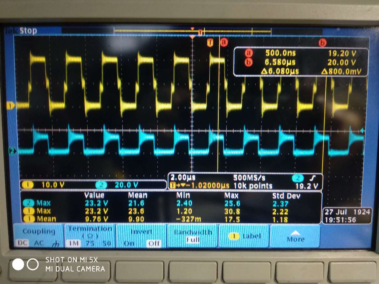
When the power is turned on, the secondary synchronous rectification is added, the waveform is abnormal, and the input current continues to rise, and the waveform is as follows:

The yellow waveform in the above figure is the transformer primary winding voltage, that is, the intermediate junction voltage of the half bridge arm. When the primary MOS tube is turned off, it is dead time and the oscillation is abnormal.
The blue color above is the secondary winding voltage of the transformer, that is, the voltage between the DSs of the synchronous rectifier.

When the secondary synchronous rectification is turned off, and the 4A load is added, the waveform is normal, the input current is stable, and the waveform is as follows:

I am very confused, why is the circuit abnormal after adding synchronous rectification?

  • An expert will get back to you shortly
  • I first tested the open-loop drive waveform as follows:

    The figure above shows the driving waveforms of the first two lower MOS tubes, and the open loop is set to 30% duty cycle.

    The figure above shows the primary 2 MOS tube drive waveforms with bootstrap and a fixed duty cycle of 30%.

    The figure above shows two secondary synchronous rectifier drive waveforms with a fixed duty cycle of 50%.

    The blue color above is a primary lower tube and the yellow is a secondary synchronous rectifier drive waveform.

    The primary 4 way, the secondary synchronous rectification 2 drive signals are stable, which is tested under the open loop, and the main power is also stable.

    The blue color above is the DS waveform of the primary lower tube MOS, and the yellow is the DS waveform of the secondary synchronous rectifier.

  • Below is the closed-loop test waveform, which, like the open-loop test above, is the drive waveform tested at no load.

    The blue color above is a primary lower tube drive waveform, and the yellow color is a primary upper tube drive waveform. The waveform is dithering and the yellow upper tube drive wave is mis-conducting.

    This is the primary two upper tube drive waveforms, the waveform is abnormal, the blue is not mis-conducting, and the yellow is.

    This is the primary two lower tube drive waveforms. The blue is mis-conducting. The minimum gate voltage of the MOS tube is 1.2V.

    The yellow picture above is the secondary synchronous rectification drive signal, and the blue is the primary MOS lower tube drive signal. The primary is mis-conducting, and the secondary is not.

    The drive waveform is abnormal and the main power waveform is also abnormal.

    Blue is primary and yellow is secondary.

    I am very puzzled. Why is the drive waveform stable when the open loop control is applied, and the drive waveform is misdirected when the closed loop control is performed?

    Also, is the drive waveform mis-conducting causing the main power waveform to oscillate, or is the main power waveform oscillating, causing the drive wave to be mis-conducted?

  • I think your transformer has large leaking inductance. During deadtime, the leakage inductor is oscillated with parasitic cap of MOSFET. The board layout can contribute the oscillation as well. If the loop is not stable, you need tune your control loop because your power stage is different from Ti power stage.
  • I am going to close the thread.
  • Ok, I found that the drive timing is incorrect.
  • The thread is closed.