This thread has been locked.

If you have a related question, please click the "Ask a related question" button in the top right corner. The newly created question will be automatically linked to this question.

LMG5200: Ringing on switch node

Part Number: LMG5200

Hello,

I am making some measurement on the design that I have and I am seeing some ringing on the switch node, can this be because dead time is too high?

The dead time is set by D2, R36, C62, R37, D3 and C61.

For the layout I tried to make as close as possible to the eval board, here is what the top layer looks like:

On all layers the copper below switch node is emptied out.

On all layers the copper below switch node is emptied out.

  • I forgot to say that it is a Class-D amplifier with 48V input that in full bridge configuration puts out 100W into 8 ohm load.
  • Hi Leo,

    I am a GaN applications engineer at TI and I am happy to help you with that. Have you observed HI and LI signals on LMG5200 input? If yes, what are the dead times? Typically, as long as you keep the dead time to be more than 10ns, they should be okay. 

    I see that you have two half-bridge for your class-D audio amplifier. Have you compared the overshoot across the two switching nodes, and are they the same? I see your layout on the top layer is okay, but it looks like your AGND pin is detoured a bit to the VCC capacitor. Also did you have your return path on the second layer closest to the top layer, and overlap with the top layer traces? This will help reduce the ringing.

    If you can upload the ringing pictures that you captured, it will be helpful as well. 

    In addition to that, are you able to separate the AGND and PGND? If not, I suggest less connection between them to avoid common source inductance.

    Thanks and regards,

    Lixing

  • Here is what layer 2 looks like:

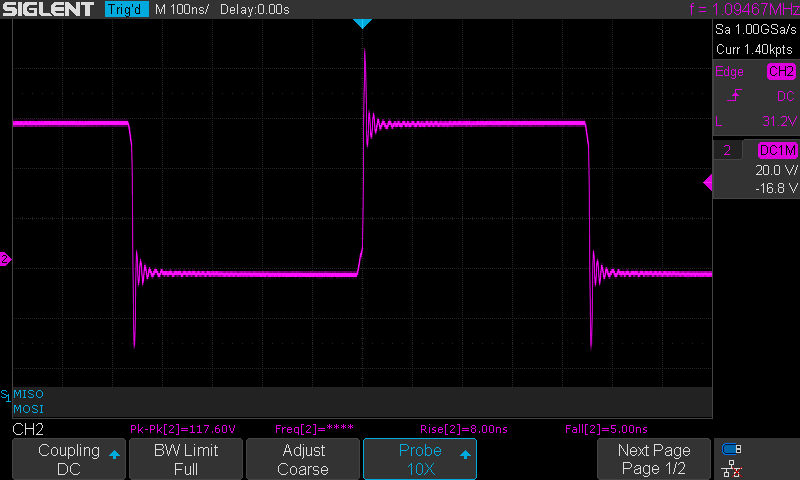
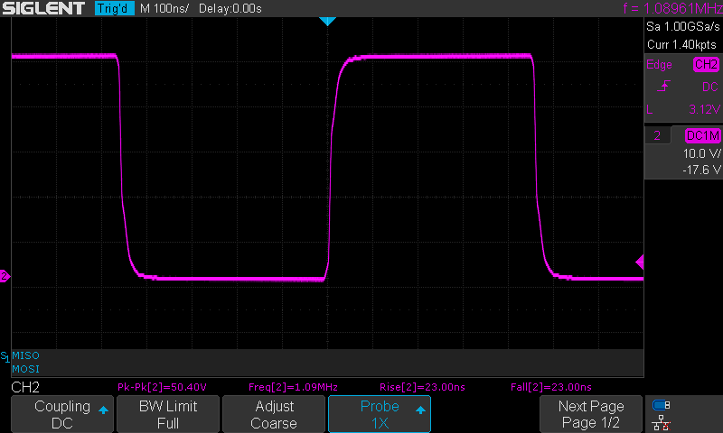
    The ringing is the same on both half bridges, the interesting thing is that I am not sure whether it is really there or not because when the scope probe is set to 10x it is there and when the scope probe is set to 1x it is not see the images:

    Scope Probe 10x

    Scope Probe 1x

    I have also changed the dead time resistors from 200 ohm to 100 ohm and the LMG5200s are getting about 10 to 15 degrees hotter. The change in dead time resistors had no affect on the ringing.

  • Hi Leo,

    The layout looks all right. The only concern is that there is no separation in layout between AGND and PGND. This may bring some issues regarding common source inductance. Besides that, could you let me know how you measured the switching node signal? It looks like you may had some parasitics brought to the measurement. The attenuation of probe is not a key thing. The major thing is how you connect the probe to the board, and also what the bandwidth of the probe is.

    Thanks and regards,

    Lixing

  • I have a ground test point on the board on which I connect ground lead. Then tip of probe to the switch node.

    It is a 200MHz passive probe. I don't remember its capacitace.
  • Hi Leo,

    Are you using the ground wire from the passive probe? Typically we do not use a group clip, and I would recommend you use the pigtail kind of test point and connection. Please take a look at the Fig. 5 of this user guide.

    www.ti.com/.../snvu461.pdf

    Usually 200MHz is also not enough to catch up the fast rising edge. Something more than 500MHz should be good but the bandwidth will not affect the noise anyway.

    Thanks and regards,
    Lixing