This thread has been locked.

If you have a related question, please click the "Ask a related question" button in the top right corner. The newly created question will be automatically linked to this question.

BQ24170: Will my board work or burn ?

Part Number: BQ24170
Other Parts Discussed in Thread: TPS5652, TPS565208, CSD17313Q2, CSD25404Q3

Hello,


First of all I want to clarify that this is my first experience in the realization of PCBs.
I am a computer engineer.

I have the idea to make a robot. For that I decided to separate my circuit board in two. One for logic and the other for energy management.
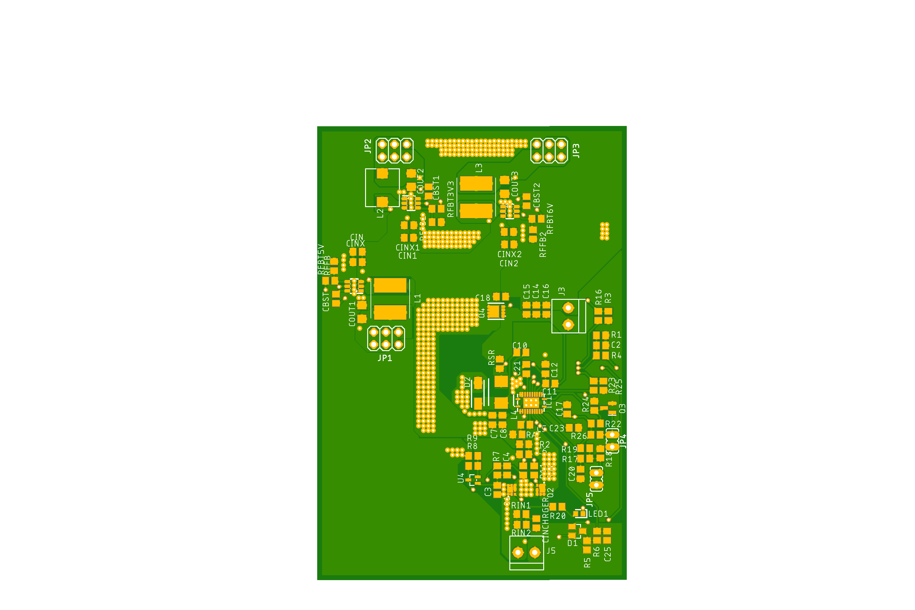
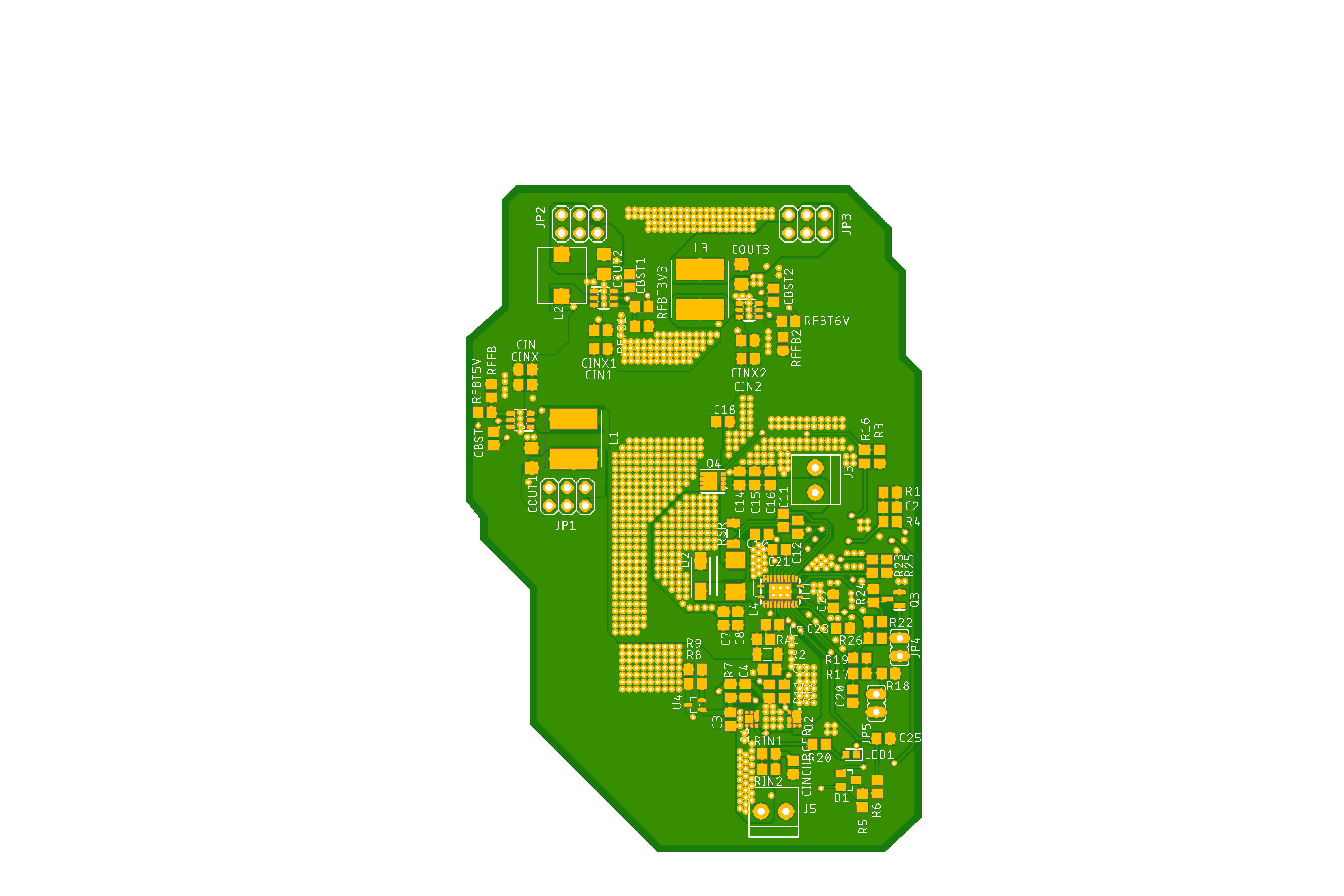
This is the second pcb that I have problems.

It serves as a charger for my batteries 3s, converter dc-dc ( tps5652) 6V, 5V and 3V3 .

I have the constraint of making a board with two layers but has a reflow oven.

I share my board in eagle format, all remarks and recommendations are welcome.

Thank you very much in advance for your help

2019-03-16_12-09-44.pdf

www.dropbox.com/.../AABXpZslODSHl0ggSNScQemoa

  • Hello Julien,

    I have reviewed your schematic. I do not see any obvious errors except for OVPSET having a resistor and capacitor instead of resistor divider. I am assuming that you used the spreadsheet at www.ti.com/.../sluc244 to properly size the components? Regarding your dropbox, I cannot access it without requesting special access through our IT department which can take a while.

    Regarding layout, I recommend following the EVM layout as documented in the user's guide: www.ti.com/.../bq24170evm-610-15v. The key components for any buck converter are the input capacitors to the converter, which will be capacitors on PVCC pins.

    Regards,
    Jeff
  • alim2.zip

    Hi Jeff,

    Thank's I have not used this spreadsheet. Great I will take a look.
    I upload a zip file. My routing is very uncertain.
    I tried to follow the desing of the EVM but can't do 4 layers board

  • Hi Julien,

    I am having trouble reading the Eagle files into Altium. Altium is asking for a .LBR file. I do not see such a file in the zip file.

    Regards,
    Jeff
  • Jeff,
    what is the name of the .lbr file you need? I will add it.

    Regards,
    Julien

    lbr.zip

  • Julien,

    I am not certain.  Altium is asking for library file, I assume for the symbols, footprints, etc using in the sch and brd files.  It might be easier if you send PDFs of the board top and bottom. 

    Regards,
    Jeff

  • Jeff,

    Here is my board

    Thank you again.

  • Julien,

    I do not think your board will burn not be as efficient and have current sensing inaccuracies. At a minimum increase the width of the trace from the inductor to D2 and move C14, C15, C16 on VBAT closer to RSR to reduce high current ripple.

    I think you could more closely follow the EVM if you used one ground plane instead of tying together with a 0 ohm resistor. This also may give more area of the power pad vias to use for heat sinking. Careful placement of the threshold setting resistor grounds and the filter capacitor grounds would be required so that switching currents do not flow through their grounds. For example, you place all of the buck converter components (including C14,C15,C15) with PGND on the end of the IC (and underneath) with pins 1, 2, 3 and 22, 23, 24 and then all other components with AGND on sides and other end (and underneath) like the EVM. You can use the power pad vias for AGND return and tie the power pad to the PGND pins under the IC.

    Regards,
    Jeff

  • Thank you Jeff for your time,

    To be honest, I did not quite understand your second paragraph. could you explain yourself please?

    I followed the other remarks you made to me. The hazardous placement of my components is due to my lack of knowledge in electronics. I want to know more.

    I also removed the components marked "open" in the BOM of the EVM. Is it ok?

    about OVPSET: I followed the schematic of the EVM :

    In my case, R9 should not be present.

    thank you,

    Julien

  • Hi Julien,

    The user guide BOM has a typo. The line under the R9 in column 3 should be removed so that both rows refer to R9. R9 for build -002 is 37.4k. A bottom resistor is required. Same for R2, R10, R22.

    Regarding my comments, if you group all of the buck converter switching components on in one area, attached to a large ground plane and then group the threshold setting and filter components needing a clean analog ground in another area on the same ground plane, the noisy switching ground will not affect analog ground components. The ground currents will choose the lowest impedance path back to IC ground. For a buck conveter, the most important components that need to be closest to the IC are in priority:
    1.the REGN capacitor
    2.the BTST capacitor
    3a.the power input capacitors that connect to PVCC- for lowest EMI
    3b. the Schottky diode on switch - for higher efficiency
    4. the output capacitors
    5. the inductor (caveat - use multiple vias to connect to the inductor but the larger/longer the trace, the greater risk for EMI).

    Regards,
    Jeff
  • jeff,

    Thank you for your patience.
    I made many changes as a result of your remarks.
    Indeed I read the BOM badly. I corrected the problem, I believe.

    Here is my new diagram, and my new PCB. Can you tell me what you think about the new version?

    I have not touched the buck part so far. And I have not merged the two ground plans yet. I mainly rearranged the tuning components and moved them away.
    I wait for your advice to be able to optimize the buck part and finalize by the masses. It's OK ?

    1374.2019-03-16_12-09-44.pdf

  • Jeff

    This is my last design. It remains 3 airwires that are unrelated ground between them 3. I would like to know your opinion.

    Thank you for everything,
    Julian

  • Hi Julien,

    I prefer an easier ground return to PGND1 for C14, C15, and C16. Can you move them closer and/or add more vias to GND? If you do remove RGND and have one ground plane, please be careful of C14-16 placement as there switching ground currents could interfere with the AGND components.

    Regards,
    Jeff
  • Hi Jeff,


    As you recommended, I think I have shortened and optimized the path to PGND1 for C14, C15, and C1. As well as grouped the two mass plans. I also tried to follow the maximum design guideline , for example as for RSR. I also join my Bom. Can you tell me if you see any abortions?

    thank you,

    I would never have done it without you.

    Julien

    3 ICSP JP1, JP2, JP3 0114_PH254-203DF118A00V 2X03 3x2 M V h 8,5 mm p2,54 M20-9980346
    3 TPS565208 U1, U2, U3 TPS565208DDCR DDC0006A_N TPS565208DDCR
    3 47µf COUT1, COUT2, COUT3 C-EUC1206 C1206 CAPACITOR, European symbol GRM32EC81C476ME5L
    1 RLF7030T-2R2M5R4 L2 RLF7030T-2R2M5R4
    RLF7030T-2R2M5R4
    RLF7030T-2R2M5R4
    2 3.3µH L1, L3 SRN8040TA-3R3Y
    3 22µF CIN, CIN1, CIN2 C-EUC0805 C0805 CAPACITOR, European symbol
    GRM21BR61E226ME44L
    1 33.2k RFBT3V3 R-EU_R0805 R0805 RESISTOR, European symbol CRCW080533K2FKEB
    1 56.2k RFBT5V R-EU_R0805 R0805 RESISTOR, European symbol CR0805FX-5622ELF
    1 68.1k RFBT6V R-EU_R0805 R0805 RESISTOR, European symbol ERJ-6ENF6812V
    6 0.1µF CBST, CBST1, CBST2, CINX, CINX1, CINX2 C-EUC0805 C0805 CAPACITOR, European symbol
    GCM188R91E104KA37J
    3 10k RFFB, RFFB1, RFFB2 R-EU_R0805 R0805 RESISTOR, European symbol RK73H2ATTE1002F
    1 0 RAC R-EU_R0805 R0805 RESISTOR, European symbol RCG08050000Z0EA
    2 0.01 RSR, R2 R-EU_R1206 R1206 RESISTOR, European symbol WSL1206R0100FEA
    2 0.047µF C4, C10 C-EUC0805 C0805 CAPACITOR, European symbol 885012207096
    6 0.1µF C5, C6, C11, C12, C23 C-EUC0805 C0805 CAPACITOR, European symbol 885012207072
    2 1 M R3, R9 R-EU_R0805 R0805 RESISTOR, European symbol RCG08051M00FKEA
    1 1.00 k R16 R-EU_R0805 R0805 RESISTOR, European symbol ESR10EZPJ102
    2 1.0µF C8, C25 C-EUC0805 C0805 CAPACITOR, European symbol VJ805Y105KXARW1BC
    1 10 R6 R-EU_R0805 R0805 RESISTOR, European symbol ESR10EZPJ100
    1 100 R17 R-EU_R0805 R0805 RESISTOR, European symbol ERJ-6ENF1000V
    2 100 k R23, R26 R-EU_R0805 R0805 RESISTOR, European symbol RK73G2ATTD1003C
    4 10µF C7, C14, C15, C18 C-EUC0805 C0805 CAPACITOR, European symbol C3216X7R1E106KST
    2 1X2-3.5MM J3, J5 1X2-3.5MM 1X2-3.5MM 3.5mm Terminal block 20020327-C021B01LF
    4 1µF C16, C17, C20, C21 C-EUC0805 C0805 CAPACITOR, European symbol GMK212B7105KG-T
    1 2.2µF C2 C-EUC0805 C0805 CAPACITOR, European symbol TMK212B7225KG-TR
    1 232 k R22 R-EU_R0805 R0805 RESISTOR, European symbol ERJ-6ENF2323V
    1 2N7002 Q3 2N7002 SOT96P240X120-3N N-channel MOSFET,2N7002 0.115A 60V 2N7002
    1 3.01M R8 R-EU_R0805 R0805 RESISTOR, European symbol CRCW08053M01FKEA
    2 3.9 RIN1, RIN2 R-EU_R0805 R0805 RESISTOR, European symbol ESR10EZPJ3R9
    1 30.1 k R18 R-EU_R0805 R0805 RESISTOR, European symbol ERJ-6ENF3012V
    2 32.4 k R24, R25 R-EU_R0805 R0805 RESISTOR, European symbol CR0805FX-3242ELF
    1 37.4 k R1 R-EU_R0805 R0805 RESISTOR, European symbol ERJ-6ENF3742V
    2 4.02 k R10, R11 R-EU_R0805 R0805 RESISTOR, European symbol CR0805FX-4021ELF
    1 4.99 k R20 R-EU_R0805 R0805 RESISTOR, European symbol ERJ-6ENF4991V
    1 402k R4 R-EU_R0805 R0805 RESISTOR, European symbol ERJ-6ENF4023V
    1 4700pF C3 C-EUC0805 C0805 CAPACITOR, European symbol 885012207090
    2 499k R5, R7 R-EU_R0805 R0805 RESISTOR, European symbol ERJ-6ENF4993V
    1 5.23 k R19 R-EU_R0805 R0805 RESISTOR, European symbol ERJ-6ENF5231V
    1 B220A-13-F D2 B220A-13-F DIOM5226X230N Diodes Inc B220A-13-F, SMT Schottky Diode, 20V 2A, 2-Pin DO-214AC B220A-13-F
    1 BAT54C D1 BAT54C SOT23 Schottky Diodes BAT54CLT1G
    1 BQ24170RGYR IC1 BQ24170RGYR RGY(R-PVQFN-N24) 1.6-MHz Synchronous Switch-Mode Li-Ion and Li-Polymer Stand-alone Battery Charger BQ24170RGYR
    1 BSS138W-7-F U4 BSS138W-7-F SOT65P210X110-3N N-CHANNEL ENHANCEMENT MODE MOSFET BSS138W-7-F
    2 CSD17313Q2 Q1, Q2 CSD17313Q2 CSD17313Q2 MOSFET N-Channel 30V 5A NexFET SON6 Texas Instruments CSD17313Q2 N-channel MOSFET Transistor, 5 A, 30 V, 6-Pin SON CSD17313Q2
    1 CSD25404Q3 Q4 CSD25404Q3 DQG_VSON-CLIP 20 V P-Channel NexFET Power MOSFET CSD25404Q3
    1 IHLP2020CZER3R3M01 L4 IHLP2020CZER3R3M01 INDPM5552X300N Vishay IHLP2020CZ-01 Series Shielded Wire-wound SMD Inductor 3.3 uH +/-20% 8.5A Idc IHLP2020CZER3R3M01
    1 LTST-C190GKT LED1 LTST-C190GKT LEDC1608X90N LED,SMD,0603,Green,6mcd,130deg Lite-On LTST-C190GKT Green LED, 569 nm, 1608 (0603), Rectangle Lens SMD Package LTST-C190GKT

  • Julien,

    I don't see any obvious errors with the components in the BOM. I suggest that the buck converter's ceramic capacitors voltage ratings be at least 1.5X higher than the expected DC voltage on those capacitors in order to account for DC bias effects.

    Regards,
    Jeff