This thread has been locked.

If you have a related question, please click the "Ask a related question" button in the top right corner. The newly created question will be automatically linked to this question.

TPS2412: Oscillations on gate

Part Number: TPS2412
Other Parts Discussed in Thread: TPS2410

Hello,

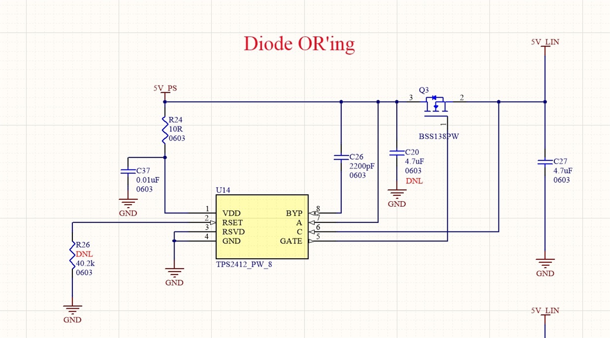
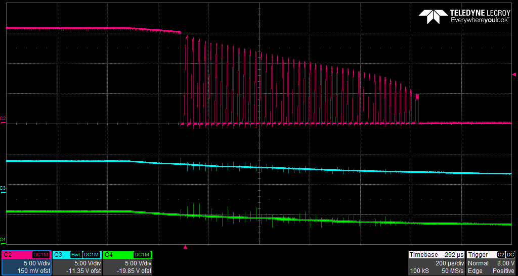
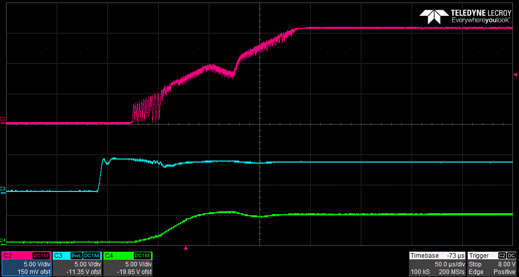
I have two standard circuits (I think) per the datasheet for this TPS2412 in parallel.  Both are supposed to pass 5V to the PCB.  One 5V circuit passes USB 5V.  The other passes a power supply 5V.   Why would the gate line be oscillating?  Pics attached. 

Power off wave form of one TPS2412 circuit

Powering on of the other TPS2412 circuit

The pink line, ch2, is the gate of the N-channel mosfet.

  • Hi Robbie,

    We will look into the issue and get back to you soon.

    Best Regards,
    Rakesh
  • Hello Robbie,

    Connection for Pin A and Pin C are reversed in customer schematic.

    Pin A has to be connected to Source of MOSFET and Pin C to Drain of MOSFET.

    Refer to the application diagram of datasheet. (attached here).

    Regards,

    Kari.

  • Hello Robbie,

    Let us know if you were able to check my reply.

    If your question is answered, click "this resolved my issue" button at the end.


    Regards,
    Kari.
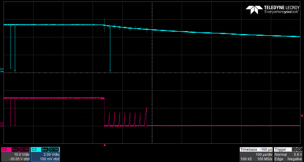
  • Thank you guys for the help.  I have reversed my FET and the system seems to be working better.  I do have a lingering question regarding the gate drive ringing and some intermittent turn on/offs.  As you can see in the attached scope capture there is still some pulsing on the gate of one of the FETs.  The power is supplied by a USB connector/cable and when I unplug it as quickly as I can I see this waveform.  The bottom trace (purple/violet) is the FET gate and the top is the 5V power coming in over the USB cable.  Is the noise on the gate and random on off transitions likely due to the mechanical interface between the cable and USB connector?  

  • What exactly does this statement int he datasheet mean?  Where would this clamp diode go and if the outputs are or'd together how would this use case be realized?

    If C falls below A by more than about 0.7 V, a small current flows out of C. Protect the internal circuits with an external clamp if C can be more than 6 V lower than A.

  • Hello Robbie,

    Regarding the random gate on/off during the time when the 5V USB input cable is removed is due to the input disturbance seen on the 5V input itself. Notice that the output is held by C27 4.7uF and input goes below the reverse turn off threshold (reverse threshold is of the order of few mV), then internal reverse comparator will turn off the gate and once the transient is gone, gate is turned on again.

    We see the gate on/off is due the fact that input is having disturbance. If you could increase the capacitance at the input (A pin) then this can be mitigated.

    Regarding the second question on "C falls below A by more than 0.7V", this scenario is not applicable for your use case. Because, even when the MOSFET is off, body diode conducts and forward voltage does not go beyond 0.7V (unless a higher forward voltage rated MOSFET is chosen).

    However, in some cases, TPS2410/11 (and not TPS2412/13) can be used to control two MOSFETs in series connected back to back. This is shown in the Figure 18 of TPS2410 datasheet under a section on "BIDIRECTIONAL BLOCKING AND PROTECTION OF C" on page 22.

    Let us know if you all your questions are answered.

    If your problem is resolved, click "this resolved my issue" button at the end.

    Regards,
    Kari.
  • Is the added capacitance just for filtering (kind of debouncing) the 5V input? Is there any kind of metric I could use in picking the amount of capacitance?
  • Hi

    Please refer to the application note to choose the capacitance: "www.ti.com/.../slva684.pdf"


    Regards,
    Kari.