This thread has been locked.

If you have a related question, please click the "Ask a related question" button in the top right corner. The newly created question will be automatically linked to this question.

REF6025: Reference noise

Part Number: REF6025
Other Parts Discussed in Thread: ADS1259

Hi,

I apologize that this topic is not related with the REF6025 directly.

Please move to proper forum if this forum is inappropriate.

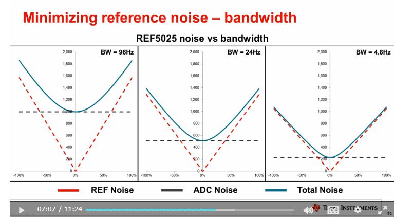
I watched the delta sigma-voltage reference training video below URL.

Below slide is shown from about 4:30.

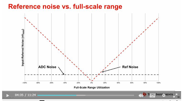
Why is Ref Noise proportional to Full-Scale Range Utilization?

I'm thinking that Ref noise is constant regardless of input signal.

Best Regards,

Kuramochi

  • Hi Kuramochi,

    From my understanding of the video. The reference noise from the voltage reference is constant into the ADC. The graph you are looking at is how to combine the inherit ADC noise and VREF noise and refer it to the input.

    Here is another document that talks about the same thing. www.ti.com/.../slyt339.pdf

    Here is another blog that discusses in more detail.

    https://e2e.ti.com/blogs_/archives/b/precisionhub/archive/2015/12/11/the-impact-of-voltage-reference-noise-on-delta-sigma-adc-resolution


    The voltage reference noise is constant but because Output Code ∝ Vin/Vref, in lower Vin voltages the ratio decreases.
    When looking at input referred noise, we are looking at the transition noise between codes. If we compare 2 different Vin with the same VREF w/ noise , we will see that the higher of the Vin will have a larger code difference from the ideal.

    For example
    Vin = 1V, 5V
    Vref = 10V
    Vnoise (exaggerated) = 0.1V
    12-b Resolution

    For 1V
    Output Code (noise) = 2^12 * 1/(10+0.10) = 406
    Output Code = 2^12 * 1/(10+0.10) = 410
    Code difference = 4 codes -> ~10mV

    For 5V
    Output Code (noise) = 2^12 * 5/(10+0.10) = 2028
    Output Code = 2^12 * 5/(10+0.10) = 2048
    Code difference = 20 codes -> ~50mV

    From this example we can see that 1V Vin will worst case see a 10mV error. While at 5V Vin will see an increased error of 50mV. This shows the linear effect of VREF noise at the input of the ADC.

    -Marcoo

  • Marcoo-san,

    I have additional questions.

    Below slide is shown from about 7:07.

    Does this "bandwidth" mean the reference noise filter cut-off frequency?

    If yes, why does ADC noise decrease depending on this bandwidth?

    Best Regards,

    Kuramochi

  • Hi Kuramochi,

    Yes, bandwidth refers to the cutoff frequency of the voltage reference and ADC.

    For the VREF the filter is determined usually by the output cap or RC filter at the output.

    In this video they refer to the ADS1259 which has a programmable digital filter.

    By changing the filter you can affect the bandwidth and reduce the bandwidth. This does come at the cost of data rate but it will reduce the noise.

    -Marcoo