This thread has been locked.

If you have a related question, please click the "Ask a related question" button in the top right corner. The newly created question will be automatically linked to this question.

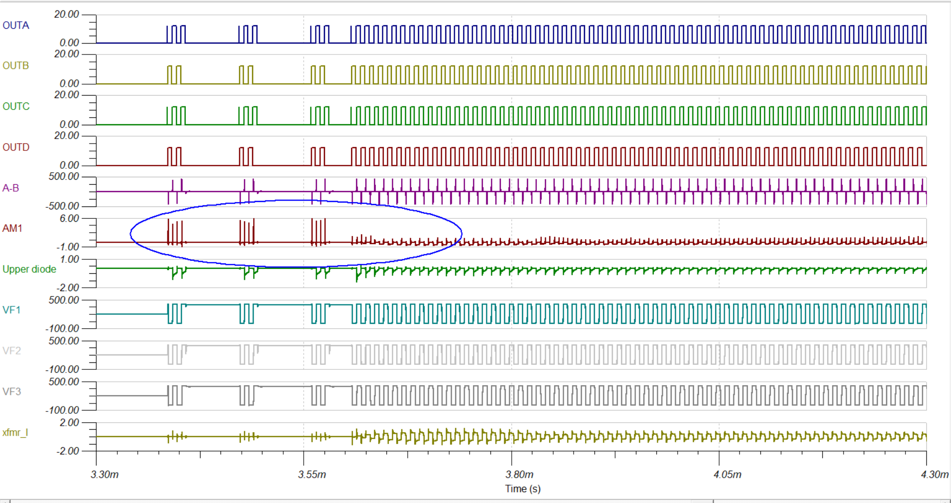
TINA/Spice/UCC28951: Q1. In which mode (burst, DCM or CCM) controller working at startup of UCC28951? because initially from 3.40m to 3.65m waveform looks abnormal in TINA TI Transient start up simulation of UCC28951. AM1 is current through Mosfet Q3, why

Part Number: UCC28951
Other Parts Discussed in Thread: TINA-TI,

Tool/software: TINA-TI or Spice Models

Q1. In which mode (burst, DCM or CCM) controller working at startup of UCC28951? because initially from 3.40m to 3.65m waveform looks abnormal in TINA TI Transient start up simulation of UCC28951. AM1 is current through Mosfet Q3, why it is much higher initially as highlighted and then reduces afterward.

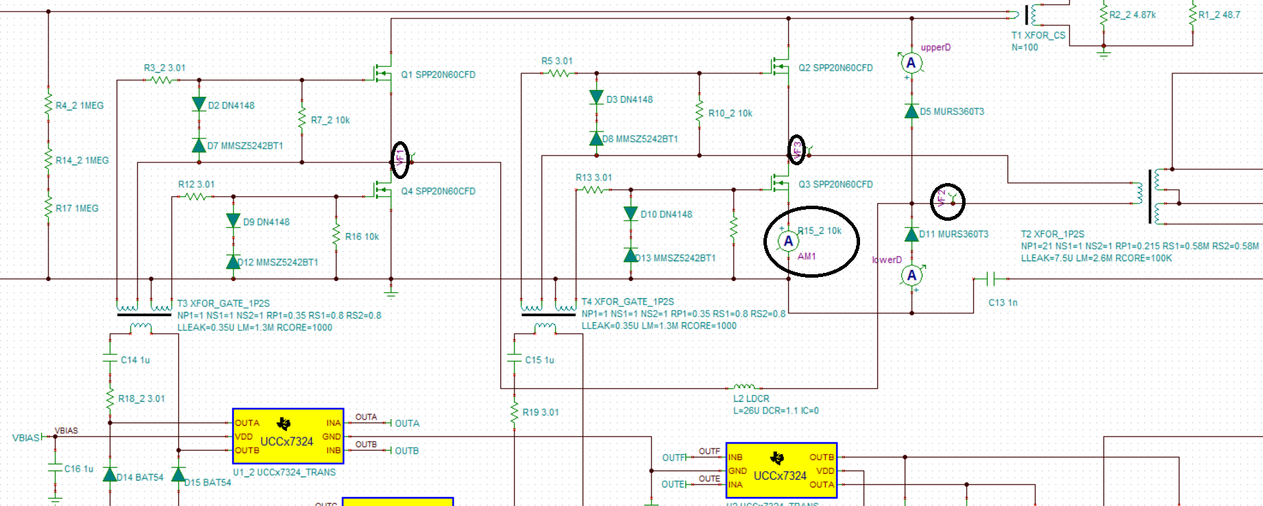
Q2.Why in simulation during startup voltage at VF1 i.e at source of Q1 and at VF3 source of Q2 Voltage is high when there is no gate pulses. (attached schematic)

  • Hello SUDHANSHU

    A1/ I re-ran the sim on my PC and got more or less the same results. The high current spikes are due to the fact that at that time the node is hard switching instead of Zero Voltage Switching. Hard switching has a much higher dv/dt rate than ZVS so the capacitive currents in the source of the device are much higher. Later on – as the sim progresses, there is enough energy available to force ZVS and the dv/dt rates reduce and so do these current peaks. One of the characteristics of the PSFB is that the PA leg, (Q1/Q4 in your schematic) loses ZVS at a higher current than the AP leg (Q2/Q3 in your schematic). If you look at the dv/dt rates a little later in the sim – around 3.6ms – you can see that QA_S (Q1_Source in your sim) is not achieving ZVS – you can see the partial change in the voltage, then the fall then the hard switch transition and the currents in this leg (AM1) are much higher than those in the other leg (AM2) which is achieving just on the borderline of achieving ZVS. The differences in the dv/dt rates are easily seen.  Please note that - unfortunately - I labelled the meter in the source of Q3 as AM2 instead of AM1 as in your sim. I used AM1 for a meter in the source of Q4.


    A2/ The voltage at the source of Q1 and Q2 was initially at about 150V when I ran the sim. I’m not sure exactly why this is so but it’s not unexpected. The voltage will be set as the input voltage increases – I’d expect that the drain-source capacitances would charge approximately at the same rate so the sources could end up at about Vin/2 or 200V. There may be leakage currents modelled which upset the balance and give you 150V instead or it may be some other effect. You could try the effect of adding some more capacitance at these sources and seeing the effect. I re-ran the sim with the SS/EN pin at 0V and the two sources settled at Vin/2.

    Regards

    Colin

  • Dear colin,

    Thank you very much for support.

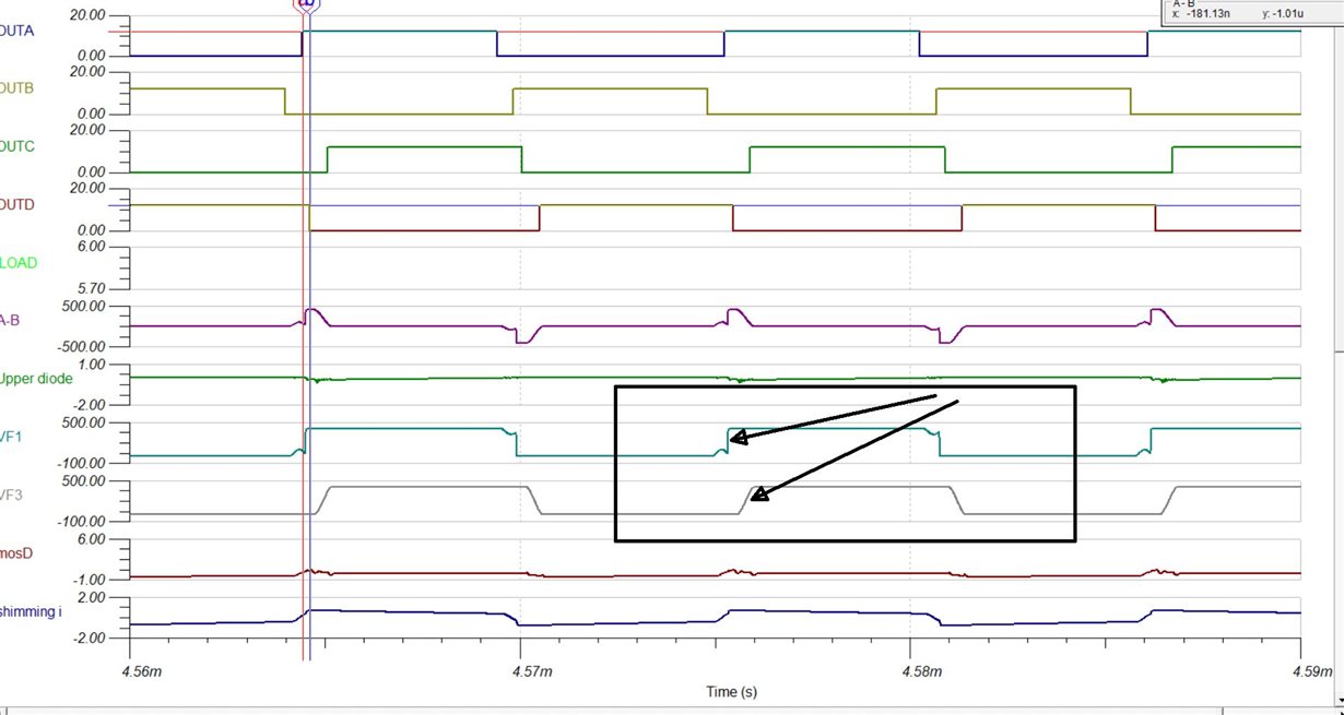
    we have one more doubt. why slope of VF3 (dv/dt) is less than VF1? (In actual board also we are getting same pattern on low load or no load).

  • Hello SUDHANSHU

    The reason is that there is less energy available to drive the ZVS transition on the PA (Q1,Q4) leg than on the AP (Q2,Q3) leg. This means that as the load is reduced the PA leg will lose ZVS before the AP leg. This is what you are seeing in the sim and on the EVM. This is a characteristic of the PSFB topology. The note at /cfs-file/__key/communityserver-discussions-components-files/196/ZVS_5F00_SubSet.docx should explain more fully. Please let me know if you need more information.

    Regards

    Colin

  • Thank you very much Colin. This answer and document attached solved my all doubts. During further exploration of this interesting controller and topology if any questions arise in my mind I will let you know.