This thread has been locked.

If you have a related question, please click the "Ask a related question" button in the top right corner. The newly created question will be automatically linked to this question.

UCC27714: UCC27714

Part Number: UCC27714

Hi Richard Herring,

We are using UCC27714 in Two-Transistor Forward Converter topology. We have used the circuit from tidrti6.pdf and attached the one which we have used.

We are observing two issues with UCC27714 

1) That the UCC27714  is getting hot when used to drive Two-Transistor Forward Converter mosfet at  400V DC 

2) That the mosfet Q1 and Q2 in DL1826-GATE DRIVER BASED ON UCC27714.pdf got hot used to drive Two-Transistor Forward Converter mosfet at  400V DC

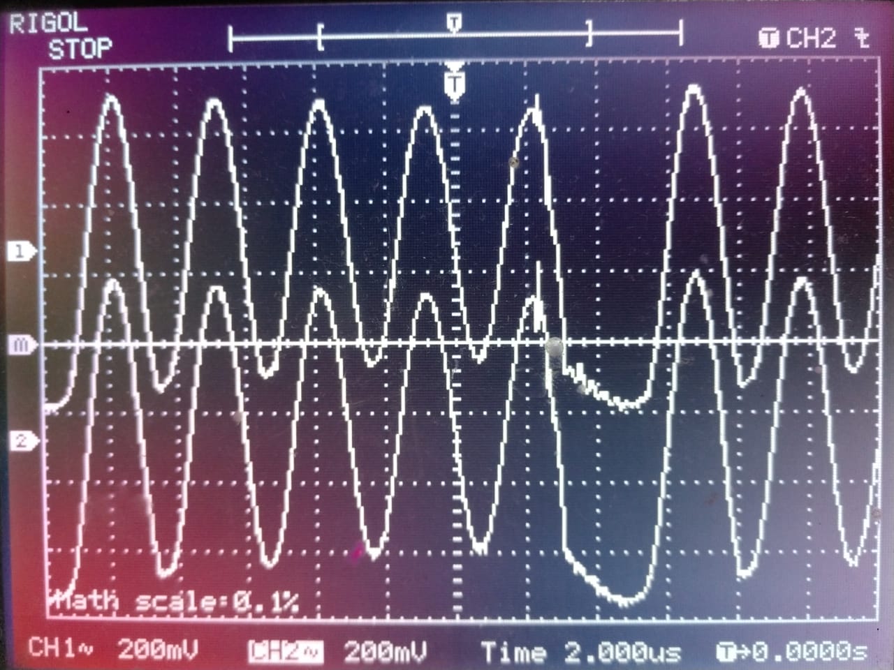
3) We are unable to see PWM signal on CRO at HO and HS while signal between LO and COM is observed to drive  Two-Transistor Forward Converter mosfet at  400V DC.

4) Please suggest which circuit we should for Two-Transistor Forward Converter topology. with components and parts numbers.

Thanks and Best Regards,

VK Verma

DL1826-GATE DRIVER BASED ON UCC27714.pdf

GATE DRIVER CKT FILL COMP.pdf

  • Hello VK,

    Thank you for the interest in the UCC27714. For the two transistor forward, there are considerations to make sure the HB to HS bias can be maintained which is why the two additional transistors and components are shown in Figure  49 in the UCC27714 datasheet two transistor forward converter circuit.

    I see the two additional switches for the HB-HS bias in your schematic, Q1 and Q2. I do see some differences in the driving signal for Q2 however.

    I have some questions regarding your implementation. I see two different signals for the HI and LI inputs. Is there some reason there are the two different signals? Usually the HI and LI are driven in phase for a two transistor forward. Are the HI and LI input signals the same timing in your circuit?

    The UCC27714 reference schematic Figure 49 has the Q2 transistor connected to the LO output of the driver. Where your circuit has the HI input. There is propagation delay between the HI/LI and HO/LO signals. The timing delay may cause some timing conflict of the Q1 and Q2 transistors and the main power FETs and switch node. Have you tried the Q2 transistor connected to the LO output?

    The purpose of the Q1 and Q2 transistors is to ensure that the HS node switches close to ground to allow charging of the HB-HS capacitor. You want to make sure the Q1 device is turned off before the high side MOSFET in the power train is turned on, to avoid timing conflict.

    For the heating concerns, there may be timing conflicts of the Q1/Q2 circuit and the power train, confirm the timing of the Q1 transistor will not conflict with the high side power MOSFET. For the gate driver IC. Review the power dissipation of the gate drive outlined in Section 9.2 of the UCC27714 datasheet. The gate drive power is determined by MOSFET Qg, switching frequency, and VDD bias voltage.

    The devices chosen for Q1 and Q2 should allow for fast switching, and Q2 voltage rating looks adequate, so these should be good choices.

    Please confirm if this addresses your concerns, or you can post additional questions on this thread.

    Regards,

    Richard Herring

  • Hi Richard!

    Thank you for your prompt reply !

    Please refer DL1826-GATE DRIVER BASED ON UCC27714.pdf, where we have provided option for providing separate or common PWM signals and in our present application we have applied common single PWM to HI and LI through R10,R11 and R14 by not mounting U4/U5, U1 R8 and R13.

    Therefore the PWM signals are in phase.

    I will do the necessary corrections as suggested by you to nullify the propagation delay and then I will share you my observations. 

    Moreover  I took this circuit from tidrti6.pdf and same is attached for your reference.

    Thanks and Best Regards,

    VK Vermatidrti6.pdf

  • SCHEMATIC1 _ GATE DRIVER PCB ON 174191746.pdfHi Richard!

    As per your recommendations I have made correction in the circuit.  Please check attached file  SCHEMATIC1 _ GATE DRIVER PCB ON 174191746.pdf , as you can see I have selected R7(R bias) = 2.2R and R9(R boot)= 2.2R and other parts are also mentioned in the circuit for your reference.

    Observations:

    1)  UCC27714  is still heating when we apply PWM signal with 60Khz @ 10 % Duty, but if we stop the PWM then heating stops.

    2) I am able to observe very noise PWM signal between HO and VSS without connecting out2 to the gate of the power mosfet.

    Please advice !

    Once again thanks for your continuous support.

    Thanks and Best Regards,

    Vk Verma

  • Hi Richard!,
    observation No 3:
    After connecting power mosfet and transformer the heating of UCC27714 is very less or nil but the boot diode and boot resistance are getting very very hot.

    Please advice .
  • Hello VK,

    Thank you for the update on the modifications and testing of the board.

    Regarding the comment on the heating of the boot diode and resistance. The possible reasons that may cause this would be excessive average current required into the HB bias supply, or maybe some timing issue with the Q1 switch and the power train.

    Can you confirm if the R12 value is 10K Ohms, which is the high side gate to source resistance. Also can you take scope plots of the Q1 gate, HS to ground, and HO to ground. Take HS and HO to ground traces with the same voltage/division scale and the same ground reference. This is to make it clear when HO is above HS.

    Is the R7 resistor in series with 12V bias, also have high temperature rise?

    Let us know if this helps resolve the concerns, or you can post additional questions on this thread.

    Regards,

    Richard Herring

  •  Hello Richard,

    I connected base of the Q2 at LO pin so that propagation delay effect can be nullified.

    yes R12=10K, and R7=2R2 is the series resistance with bias.

    In this present configuration Q1 and D1 are heating but not UCC27714.

    I have attached  scope trace where Channel 1 is between (HO and GND) and Channel 2 is between HS and GND, both are at the same scale and taken when transformer is connected. 

    Kindly suggest some reference circuit with parts values mentioned which was tested and running in the two transistor configurations. So that I can start with this.

    Thanks and Best Regards,

    VK Verma


  • Hello VK,

    Thank you for the update on the testing. I have some comments about your latest schematic, and the UCC27714 Figure 49.

    Q1 drain needs to be able to pull down the voltage on Q2 Vgs. The R9 resistor needs to be moved to be between C12 and D3/Q1/Q2 connection.

    Since Q1 needs to be able to pull down Q2 Vgs, increase the R7 diode resistance to higher values to limit the current. Try at least 20 Ohms for R7.

    I have some question about he scope plots, Is the scale as shown as 200mV/division? I would expect high voltage waveforms.

    I would expect more square wave waveforms, but if there is no load, or the secondary load circuit is not connected, this would affect the waveforms.

    Can you confirm the voltage scale, and record waveforms of Q1 VGS, HO to ground, and HS to ground with the same voltage scale and ground reference location.

    Let me know if this helps, or you can post more questions on the thread.

    Regards

    Richard Herring