This thread has been locked.

If you have a related question, please click the "Ask a related question" button in the top right corner. The newly created question will be automatically linked to this question.

BQ76930: BQ769x0 Unused Cell Connection

Part Number: BQ76930
Other Parts Discussed in Thread: TIDA-00792, EV2400, BQ78350, BQ76200

Hi everyone. I have a few days reading this forum, found several themes, but the information is divided. The question is how to properly connect unused cells, when the number of series cells in the battery decreases. I used the BQ76930, a battery 8S, in accordance with datasheet on BQ769x0 (SLUSBK2H ) need to short a cell VC3+VC4, and VC8+VC9.

I fulfilled those conditions. 

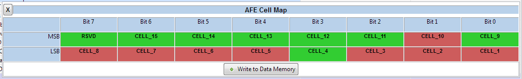
Here's mine AFE Cell Map

Then in one of those on this forum, I've read, that unused components can distort measurements.I have removed unused components according to the following document. Here is a picture from the document TIDA-00792 (TIDUCN1), page 5, paragraph 2.2.1. 

As a result, the balancing on cell 5 and cell 10 stopped working, I tested the balancing command with command 0x001B. Now I ask you to turn to the scheme.This is how it looks initially.

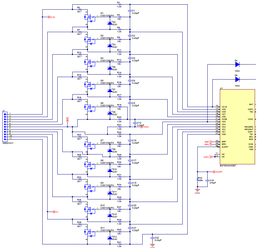
And so after revision in accordance with the document  TIDA-00792 (TIDUCN1). 

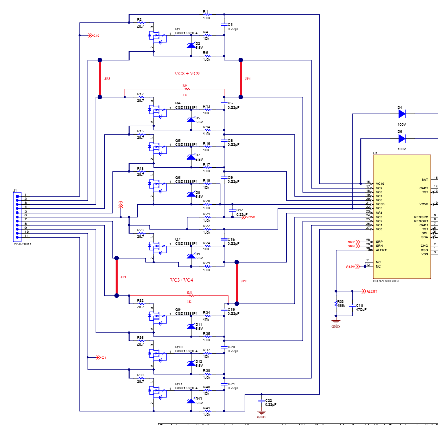
I deleted components R28,Q8, D10, R30, R31, C17 for point VC3+VC4, and components R7, Q2, D3, R9, R11, C2 for point VC8+VC9. Then I set the jumpers JP1+JP2 for point VC3+VC4, and jumpers JP3+JP4 for point VC8+VC9 (As jumpers were 0 Ohm resistors installed instead of capacitors C2 and C17, respectively). Cell balancing vc5 and VC10 still didn't work. 

Then I installed the resistors R9 and R31, remove jumpers JP2 and JP4, and balancing has work. But it contradicts the document TIDA-00792 (TIDUCN1), since now there are no jumpers on the terminals of the chip, and there are filter resistors R9 и R31.Will not do this error of measurement? Advise how to connect correctly.

  • Hello Alexey,

    Are you using EVM board to run the test or your own board? Did you send 0x1B to register 0x01 and 0x02 register ? Have you test to enable the cell 5 or cell 10 only for balancing.

    As this Friday is US holiday, we may have late response then.
  • Hi, Jessica, thanks for your prompt reply. We use our PCB. To run the test, I use the command 0x001B in BQ Studio, we using the EV2400 programmer. The problem is that balancing on 5 and 10 cells did not work when removing unnecessary components in accordance with the document TIDA-00792 (TIDUCN1). In case you leave the resistors R9 and R31, and remove the jumpers JP2 and JP4, everything works fine.

    Even in this thread it is recommended to leave the filter resistors e2e.ti.com/.../571588 .

    But it contradicts the document TIDA-00792 (TIDUCN1), page 5, paragraph 2.2.1.

    I want to understand how it should be done right in the end.

    Congratulations on the holiday, will wait for a response.

  • Hello Alexey,

    So you also have BQ78350 on board, and use cell balance toggle for the balancing test right ?

    the filter resistor is need for the lower channel's , we will check the impact on the upper cell balancing then.
  • Hello Jessica. Yes, of course, as a control chip used BQ78350, to control MOSFETs used driver BQ76200. The basis is your EVL Board`s and other examples of your projects on a series of BQ769x0 and BQ78350.

    When we short the cell inputs (VC3+VC4 and VC8+VC9 in our example), we connect two filter resistors, and two inputs of the BQ769x0 chip connected in parallel, to one battery cell. I'm worried that it might affect the accuracy of the measurements, and possibly cause a slightly faster discharge of the cells connected to this parralel inputs?

  • Hi Alexey,

    It looks like your AFE Cell Map is set up correctly. You should remove R9 and R31 - these should not be connected.

    The problem with the Cell Balance Toggle command (0x001B) is that it does not reference the AFE Cell Map. It will simply toggle the odd cells and the even cells without knowing how things are connected externally. For your configuration, I would avoid using this command.

    To see the cell balancing with a reduced cell count configuration using the BQ78350, you will need to simulate the balancing conditions by applying a charging current and raising the cell voltages past the cell balance threshold voltage while applying different voltages to each cell input.

    Best regards,
    Matt
  • Hi Matt, thanks for your reply. Now I will check the work of balancing, using your advice. Jumpers on the outputs of the chip (in my example they are marked as JP2 and JP4) are necessary, or can we do without them?

    Let me ask one more question. If we use BQ76930 for configuration in 6S mode, we must short the cell VC3 with cells VC2 and VC4, and cell VC8 with cells VC7 VC9 respectively.
    Let's take cells VC3+VC2+VC4 for our example.
    Each of cells has its own filter components, mosfet and bypass resistor. Shorting the inputs of the cells together, we essentially get one cell instead of three.
    The unnecessary components of some two cells we need to remove. The components of one of the three cells we have to leave. Components which of the three cells is better to leave?

  • Hi Alexey,

    Yes, JP2 and JP4 should be installed when reducing the number of cells to 8.

    For the 6S case you describe, it should not matter which cell you leave the components for since you will be shorting the VC2,VC3,VC4 pins and the cell connectors for these cells.

    Regards,
    Matt
  • Hi Matt. I checked the balancing by artificially causing an imbalance of 4 and 8 cells, I removed the resistors R9 and R31, re-installed JP2 and JP4, and checked the work of balancing on the outputs of the BMS VC5 and VC 10. Balancing really works, thanks for your advice.