This thread has been locked.

If you have a related question, please click the "Ask a related question" button in the top right corner. The newly created question will be automatically linked to this question.

LMG1210: PCB Layout & TI Vault connection

Part Number: LMG1210

Hi,

I'm in the process of building a class D amplifier using the new LMG1210 drivers. (I'm probably paying too much for the op-amps, feel free to suggest alternatives). It operates from a 500kHz PWM signal using a series of opamps. I'll include the schematic below.

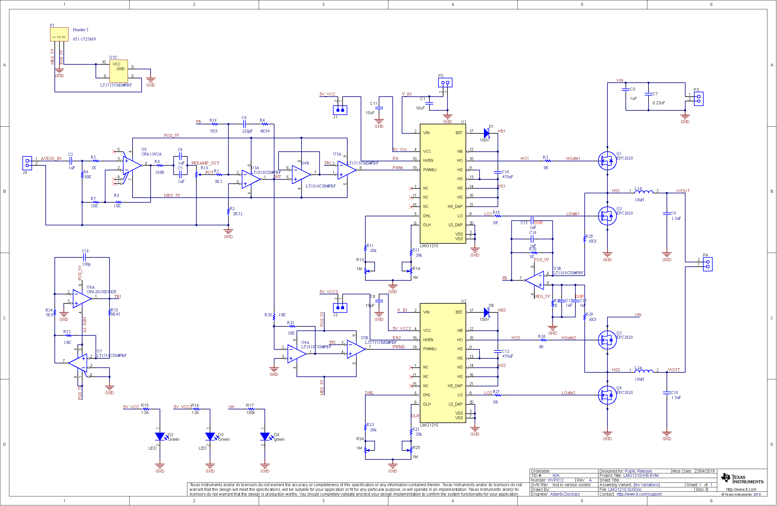
I used the schematic provided for the LMG1210 evaluation board and modified it for my design. I'm running in to some issues though connecting to the Texas instruments altium vault for the footprints when I want to create my PCB. The footprints for all components that were originally on the schematic are unavailable due to "No connection to the vault".

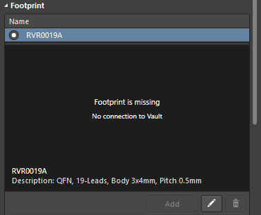
How can i connect to the vault to use these footprints?

I plan to follow the same layout as the evaluation board but because my output stage is BTL instead of single ended, i'm unsure whether to place the second leg next the the first leg like the schematic or parallel. I'll also place the inductors on the top instead of the bottom of the board.

  • Hi Dylan,

    Thanks for reaching out on LMG1210 Design Files and welcome to e2e!

    The vault is for internal use however for external use you can follow the steps below to access each individual component's footprint manually.

    Let me know if you have any more questions or this method does not work for you.

    • Open new project with Schematic and PCB open.
    • Select Design -> Make Integrated Library
    • Then Save Integrated library
    • Open component 'properties'
    • Change source to newly made integrated library
    • Manually select design item ID with correct component name
    • (Make sure it doesn’t default back to the Vault)
    • (Make sure footprint is available in the footprint properties page)
    • Finally import footprints into pcb.doc