This thread has been locked.

If you have a related question, please click the "Ask a related question" button in the top right corner. The newly created question will be automatically linked to this question.

UCC21222-Q1: Source & Sink Current(Ioa+/Iob+, Ioa-/Iob-)

Part Number: UCC21222-Q1

Dear, Sir.

My customer is evaluation UCC21222-Q1 for their system.

At this time, They are asking following topics.

Please give your advice.

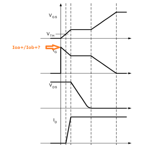
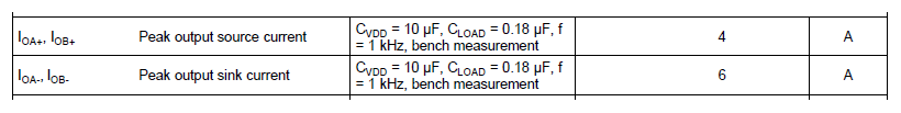
1. Source & Sink Current(Ioa+/Iob+, Ioa-/Iob-) are defined on the

    datasheet as typical. To calculate the gate charging/discharging time

    min/max would be significant, I think.

    Is it possible to clarify min/max source & sink current?

2. What is the main factor to create above variation?

    Accuracy of the internal current source?

3. I wonder Source & Sink Current(Ioa+/Iob+, Ioa-/Iob-) will keep

    to complete the charging/discharging for Qg of external FET?

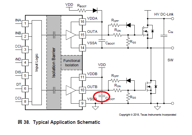
4. If Gate & Source was shorted on lowside FET(Source = GND),

    Is there any damage on UCC21222-Q1?

Best Regards,

H. Sakai

  • Hi Hideyuki-san,

    Thank you for promoting our drivers, my name is Mamadou Diallo from the High Power Driver's group.

    1&2) The specified 4A/6A drive current capability of this and any other gate driver in general is taking during a very specific time of the source/sink transient currents at the specific conditions in the datasheet. Drive current will vary and is influenced by many factors including bias cap, PCB layout, external gate resistance, etc... I discuss a bit more on this separate thread below:
    e2e.ti.com/.../2885286

    Additionally, the tech below from my colleague discusses how to calculate and determine Ioh and Iol.
    www.ti.com/.../slla387.pdf

    3) I am not sure I understand the question here. Are you asking whether 4A/6A will be sufficient to charge/discharge an external FET of gate charge Qg? If so, what is the total gate charge?

    4) What would the benefit of shorting the gate and source for low-side? What are your trying to achieve by doing so? Can you help understand the thought process?

    Thanks in advance for the additional information.

    Regards,

    -Mamadou
  • Dear, Mamadou-san. 

    Thank you so much for your valuable information. I would like to make sure several. 

    Please give your advice. 

    1&2) 

    I understand the source/sink current is influenced by many factor. 

    However, RNMOS/ROL on internal transistor will be one of major factor. 

    I wonder typ. 4A/6A specification are reflected on the worst case RNMOS/ROL

    (Highest & lowest)? 

    If not, Is it possible to clarify min. or max as the reference? because min. will be

    important to estimate power dissipation, etc. 

    3)

    I wonder Ioa+/Iob+ mean the peak as below? 

    4)

    I understand the stored energy on CBOOT will be limited during gate-source short in high-side case. 

    I wonder the situation in low-side case is same as high-side case? 

    There is the possibility that gate-source short would be happened during manufacturing process 

    such as miss-soldering, etc. So the customer is asking such. 

    Best Regards, 

    H. Sakai

  • Hi Sakai-san,

    1&2) The outputs are designed such that the internal pull-up and pull-down FETs will saturate around 4A and 6A respectively. The peak current will vary slightly with process, temperature, and voltage, but does not change significantly. The typical Rdson values do not change significantly and should be adequate for power dissipation calculations.

    3) Yes, Ioa+ and Iob+ peak during the initial switch from low to high, and slowly fall as Vgs rises, and Vds falls. These currents go to ~0A when the gate is fully charged.

    4) You are correct that if the gate was shorted to the source, the high side Cboot would quickly drop below the UVLO threshold and the output would turn off. The low-side, however, typically is directly powered from some kind of regulator. This output is more vulnerable to damage if the gate is shorted to the source and the regulator is capable of maintaining the VDD voltage at a higher input current. It is important to ensure that this short does not happen.

    If this helped answer your question, could you please press the green button? If you have more questions, feel free to keep asking.

    Thanks and best regards,

    John

  • Dear, John-san. 

    Thank you so much for your valuable advice. 

    4A/6A typical source/sink current capability is defined on the datasheet. 

    1. The minimum capability will be important for the customer. 

        Is it possible to assure the minimum value? 

    2. If can't assure, 

       Is it possible to show the minimum value which your obtained at qualification

       test for UCC21222-Q1? It will be good reference for the customer. 

    Best Regards, 

    H. Sakai

  • Hi Sakai-san,

    1. I'm not sure if we can assure the minimum value. I've reached out to our internal team to see what data we have.

    2. I'll need some more time to look through our data. I'll update you once I find out more information.

    Can you explain more on why this number is more important? Is there a particular ambient temperature that's of most concern here?

    Thanks,
    John
  • Hi Sakai-san,

    Our min peak source/sink currents are as follows:
    2-A minimum peak source
    3-A minimum peak sink

    Please let me know if you have any other questions. If not, could you please press the green button?

    Thanks,
    John