This thread has been locked.

If you have a related question, please click the "Ask a related question" button in the top right corner. The newly created question will be automatically linked to this question.

UCC27523: UCC27523 USING PROBLEM

Part Number: UCC27523

Hi all,

one of my customers has one  problem about UCC27523,and it follows as below:

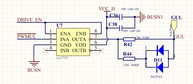
UCC27523 can not output high level, and the output voltage is lower than -2V. whether this can cause damage to the chip ? and what is the main reason which can cause no high level output disability?

Thanks a lot!

  • Hello,

    Thanks for your interest in our device, my name is Mamadou Diallo, from the High Power Drivers group. I will help address your concern.

    I have couple of comments/questions about the schematic. Can you confirm the values of R42 and R44? It looks like the 51-Ohms on the turn-on path and 100-Ohms on the turn-off path. That seems very high to me, most applications generally need no more than 10-20-Ohms depending on dv/dt and switching frequency. WHat is the expected dv/dt and switching frequency? Additionally, you would typically want have lower impedance on the turn-off path (as little as possible) than on the turn-on path to minimize losses and control the rise/fall times of the FET by tweaking R42. I assume you're driving a MOSFET, what is the total gate charge? can you verify?

    Can you also confirm values of C38 and C36? I want to make sure the driver is properly biased.

    Once those details clarified, we can start with a sanity check, with the driver(s) removed from the pcb board and by itself, do the output go high with input low and EN high (inverting driver)? Can you verify? I want to make sure that the driver is not damaged, you can do this on a separate board or on bread board just for sanity check.

    Also which package are they using? SOIC or the MSOP? If MSOP, remember the power pad is electrically connected to GND of the device so make sure no VDD vias (or no other connections except GND) right underneath the driver.

    If the driver(s) are OK, then placed on the customer board, can you please share the supply voltages measured directly from the VCC_H pin of the driver in question?

    Also what does your input signal look like? frequency? Vpp? Can you measure PWMUL, EN directly at the pins of the driver?

    Thanks for the additional information.

    I look forward to hearing from you.

    Regards,

    -Mamadou
  • Mamadou:
    Thanks for your help!
    I would answer your question:
    (1)R42=51-Ohms,R44=100-Ohms;
    (2)This chip (UCC27523)is dring a IGBT(FS20R06W1E3/20A/600V);
    (3)C38=C36=1uF;
    (4)After damaged with the reason I have'nt know ,these resistors of this chip just like this:
    1.VDD-ENA:58.52k-Ohms
    2.VDD-INA:197k-Ohms
    3.VDD-GND:0.972M-Ohms
    4.VDD-INB:200.2k-Ohms
    5.VDD-OUTB:1.959M-Ohms
    6.VDD-ENB:98.5k-Ohms
    7.Vf(OUTA-VDD):0.495V(Diode drop,in order to just the PMOS inside)
    8.Vf(GND-OUTA):0.498V(Diode drop,in order to just the NMOS inside)
    (5)the supply voltages VCC_H comes from flyback power;
    (6)PWMUL pull up,EN pull up,the OUT goes down,if PWMUL pull down(the damage chip),EN pull up,the OUT stay low,I don't know why;
    (7)Question:Are there any reason can damage this chip?the supply over voltage or OUT goes below -2V and?
    Tt seams that the NMOS and PMOS in this chip have'nt demaged yet but OUT can't go high any more,can you tell me why?
  • Hi Hongwei,

    Thanks for the additional information.

    Few comments from your answers.
    -Please reduce R42 and R44 that is way too way for most gate drives as this is only slow down the rise/fall times of at the gate and increase switching losses. You want minimal resistance on the turn-off again consider 0-5 Ohms and on the turn-on path 5-10Ohms are generally adequate depending on switching frequency.

    -As far as C38, C36, 2 ceramic (X5R or X7R) capacitors of 0.1uF and 1uF work best with our drivers.

    -IN your previous thread description, you mentioned that Vout is lower than -2V, what is the value measured? Was -2V for a short period? or extended period >300ns? Can you confirm or share waveform?

    -The OUTx shorting to GND could be related to many things transients from the flyback on the supply voltage exceeding the abs max and causing excessive power dissipation within the driver. You may add clamping diodes placed very close to the driver's supply pin to protect against such transients.
    OUTx shorting to GND can also be due to noise on the gate of IGBT damaging both the IGBT and driver or as you mentioned transients higher the -2V capability of the driver. Can you verify that the IGBT is OK or is it also shorted? To prevent this, you may also add clamping diodes to help prevent such events.

    -Additionally, I noticed the load is 200nC gate charge which is pretty heavy. If operating at higher frequencies, the driver will dissipate lot of power to delivery the peak current to turn-on/off the load. This power dissipation will create a rise in temperature at the junctions of the driver, if this rise in temperature exceed the driver's rated junction temperature, it can also damage the driver. Can you confirm your switching frequency?

    Can you please place a different driver and share scope shots during normal operation?

    Regards,

    -Mamadou
  • Mamadou,

    Thank you!

    I would like to add some information that we can make it clear.The switching frequency of IGBT is 10kHz.I have'nt captured -2V in OUT,But as it refer to the UCC27523 datasheet in page 6(Absolute Maximum Ratings OUTA&OUTB would be -2V to VDD+0.3V).I guess this chip will be damaged if this situation occur.In additonal,the IGBT is ok after this chip(UCC27523)damaged,I changed this chip,this circuit works again.The Gate to Emitter between IGBT is ok also.In the next,I will try to capture this signal in OUT if this situation happens again.In most time,this driving circuit works well,but in whole machine test,I have damaged several chips with the reason that I don't know why.I analyze this damaged thip,I found that the PMOS and NMOS inside have'nt demaged yet and the resistors seam to be ok(refer to my test result in last reply).I want to know how to just witch part of this chip was damaged inside,than I can analyze it.

    Hanping Lee 

    From ShenZhen

  • Hi Hanping,

    Thanks for the additional information.

    Please accept my e2e friend request where I can follow up with you via email.

    We can continue the discussion there.

    IN the meantime, I will mark this thread as resolved and close it.

    Thanks.

    Regards,

    -Mamadou