Hi all,
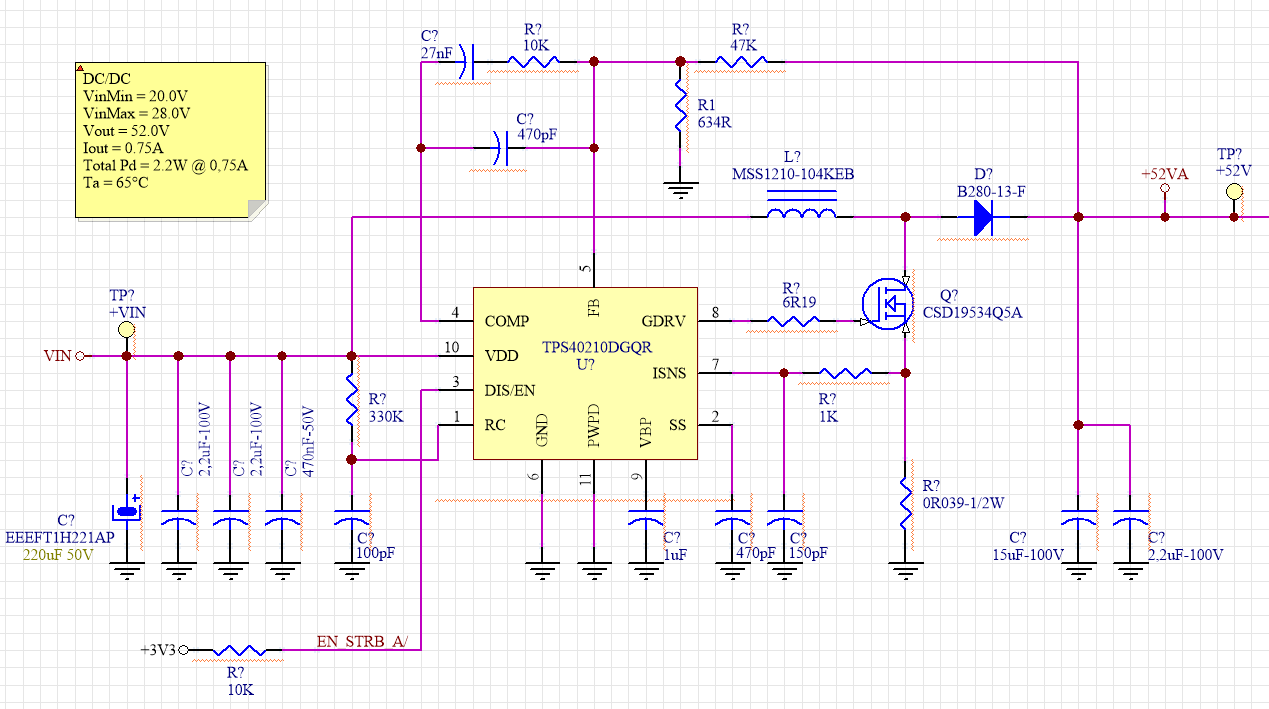
I have done a step-up with a TPS40210DGQR: Vin is 24V nom, and Vout is 52V, 0,75A nom (attached image).
I must to change dinamically the output voltage, from about 44V to 63V. To do this I would like to change R1 in order to increase or decrease the vout.
My issue regards the phase margin.. If I change the R1 value, It could be that I must to change the compensation network too, in order to keep the correct phase margin.. But I can't change dinamically the compensation network..
I tried to change the value of R1 into the webench Power Designer, then I done some simulations and trace the bode diagrams. My target is: any changing of R1 cause a permissible phase margin change. In the proofs that I have done the phase margin is always the same.. How it's possible?
The principal value of R1 are:
- 750ohm for 44V, about 100W;
- 634ohm for 52V about 100W;
- 520ohm for 63V about 100W.
With these value, I have some dangerous configuration?
How can I verify these situations?
Thanks in advance, best regards,
Diego.