This thread has been locked.

If you have a related question, please click the "Ask a related question" button in the top right corner. The newly created question will be automatically linked to this question.

BQ76200: BQ76200 SCD mos short

Part Number: BQ76200

Dear  All:

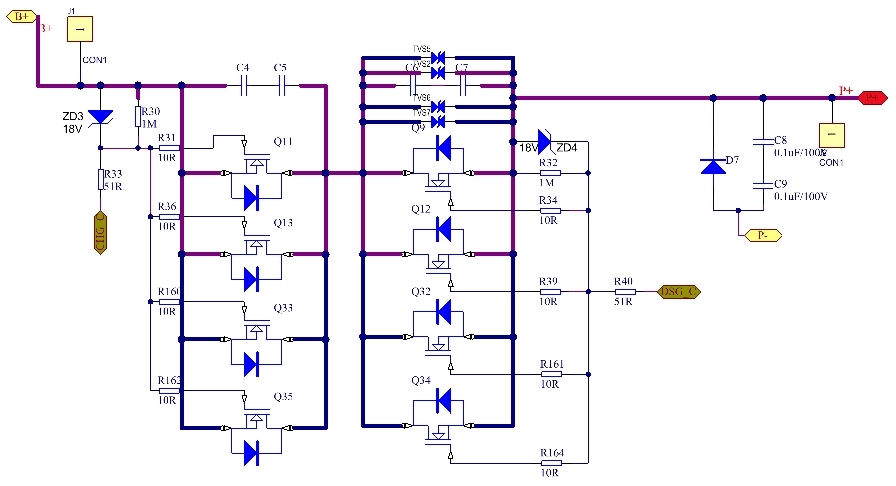
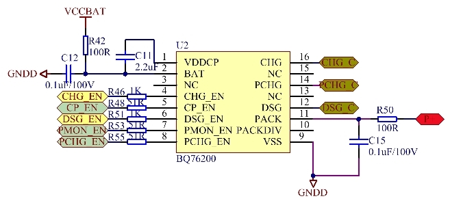
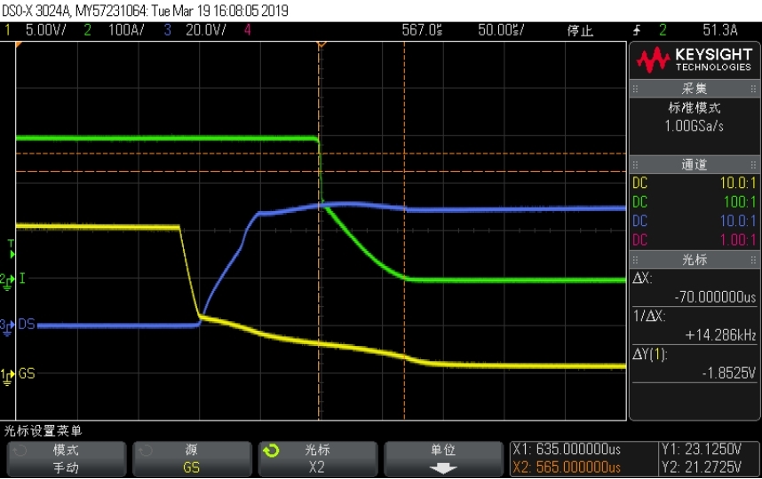
     I  use the BQ76200 to drive the High side mos in the BMS application, I find the discharge MOS  is often short  in the SCD test that the SCD current value is  1000A . As show below  is the schematic and test wave.  I find the Miller platform time is too  long.  Can you help me  to solve the issue , Thanks~

  • Hi Bill,
    C15 is too large, it will slow turn off as the load on P+ discharges C15 through R50. DSG pulls to the PACK pin so the discharge FET operates in source follower mode during the extended transition time and heats the FET. Too much heat and the FET fails. Use a small value for C15, possibly a TVS for transient protection for the pin while providing lower capacitance.
    C12 may need to be reduced to allow the part to follow load transients on B+, not a concern for DSG turn off but for load variation of B+.
    R30 and R32 provide a heavy load on the charge pump, typically these are recommended as 10M.
    You might see discussion of these items and others in the application note www.ti.com/.../slua794.pdf
  • Dear WM5295:

    I have modify the SCH as your advice, but the DSG fall time is still 73us , I see your test report the 4 MOSFET DSG fall time is only 43us, How do

    i change the circuit or add the circuit to reduce the DSG fall time. in my application, there are SDC current 1000A & Pack capacity 28AH ,

    Thanks~
  • Hi Bill,
    The circuit construction, FET characteristics, board parasitics or component tolerances must be different from the apnote test circuit. The current magnitude may have an effect also.
    With the internal resistance of the DSG pin and the careful drive of the bq76200 DSG to the PACK pin, faster turn off might be achieved with an external driver such as figure 13 of http://www.ti.com/lit/slua618 or its P-ch FET equivalent, by biasing PACK pin slightly below PACK+.
    As you consider faster switching, remember Ldi/dt response of the circuit. Since I is large and you are decreasing dt, the voltage transient may be come large. You may encounter a tradeoff between faster switching with voltage transient and a more durable FET arrangement.