This thread has been locked.

If you have a related question, please click the "Ask a related question" button in the top right corner. The newly created question will be automatically linked to this question.

WEBENCH® Tools/UCC28742: MOSFET selection for Valley Switching

Part Number: UCC28742
Other Parts Discussed in Thread: TL431, UCC28600, UCC28C42, UCC25600

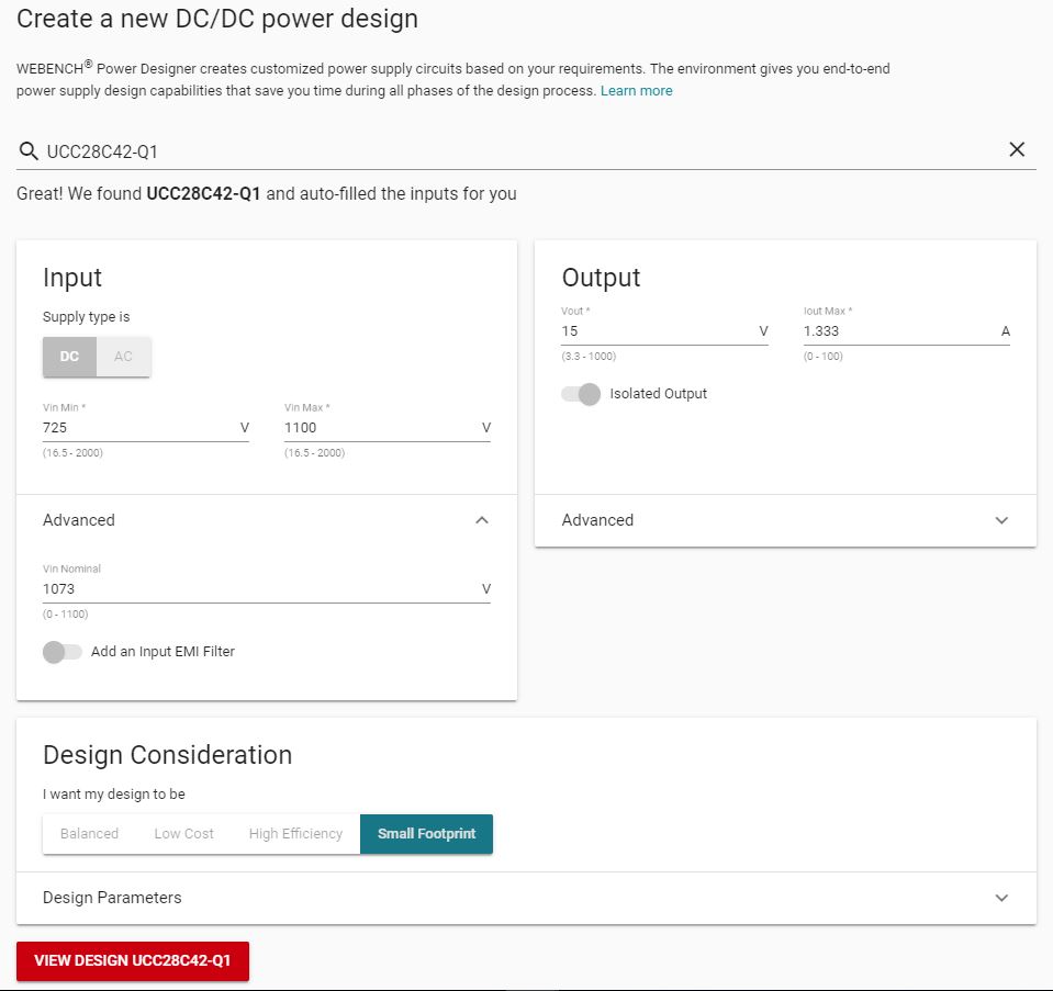
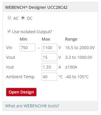
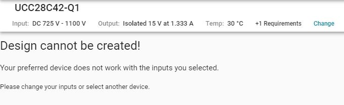
Tool/software: WEBENCH® Design Tools

I am having a hard time finding a MOSFET for the UCC28742 that will allow for valley switching.
How critical is it to achieve this?
What are the side affects of not valley switching besides lower efficiency and more power dissipated by the MOSFET?

Do you know of any MOSFETs that will better achieve valley switching?  So far even with $40 parts, I can not achieve this and be within the current rating of the MOSFET.
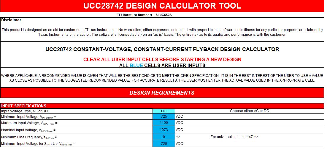
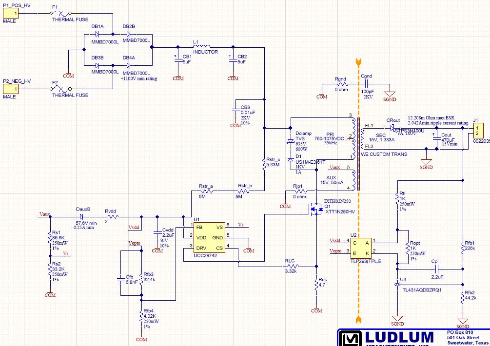
MOSFET Switch, Q  
Reflected Voltage, Vreflected = 640.0 V Variable definitions refering to the diagram on the sheet of SCHEMATIC AND BoM  
Leakage Spike Voltage, VLK =   416.0 V  
Required Drain to Soure Voltage Rating , VDSrated = 2156.0 V  
Leakage Spike Voltage / Reflected Voltage, Ratio = Vlk / Vreflected  0.65   User input and initially around 0.5 to 0.7  
MOSFET Rated Drain to Source Voltage, VDS = 2500 V    
Output Capacitance of Selected MOSFET, COSS = 77 pF Design will not Valley Switch
Drain to Source On-Resistance of Selected MOSFET, RDSon = 40  
MOSFET Fall Time, tf = 39 ns  
MOSFET Turn Off Delay Time, tDoff = 132 ns  
MOSFET Total Gate Charge, Qg = 65 nC  

Regards,
Clint

  • I am not sure why you are having issues with Valley switching?

    Could you provide schematic and power levels?

    Could you also take waveforms of the Aux winding, Drive Pin and Current Sense pins so we can see where the device is actually switching?

    Regards,

    Mike
  • I do not have waveforms to view at the moment, because I am still in the process of sorting out the correct components using the design tool.
    Once I have these correctly set, I will move to layout and PCB manufacturing and test, but I want to make sure I have setup the design correctly.

    Currently, I can not find a MOSFET to achieve valley switching at the current level needed.
    The design takes a DC input voltage (725V to 1075V) from a large capacitor bank as the input.
    The output needs to be 15Vdc at 1.3Amps.  The output voltage range during operation and various load states must remain between (14.5V to 15.5Vdc) with the typical value being 15Vdc.

    One thing I think I need to look at is revising the Vaux turns since I originally thought I'd just need 40 turns just like the secondary to have a 15V aux, but this calculator is showing I need more like 65 turns which is quite a bit more?

    I am also looking at a startup circuit to allow the circuit to start up quickly.

    UCC28742 DESIGN CALCULATIONS
    The Values Entered by the User on the DESIGN INPUT Page are Used in the Design Calculations
    ALL Gray CELLs from BLUE CELLS ARE USER INPUTS - changes only made to BLUE cells
    INPUT
    Input Voltage Type AC or DC: DC User Input Values From Design Input Page
    Minimum Input Voltage  VINPUTmin = 725 VDC
    Maximum Input Voltage VINPUTmax = 1100 VDC
    Nominal Input Voltage  VINPUTnom = 1073 VDC
    Minimum Line Frequency  fLINEmin = 0 Hz
    Minimum Input Voltage for Start-Up VINPUTrun = 720 VDC
    Minimum Peak Bulk Input Voltage  VBULKmin = 725.0 V  
    Maximum Peak Bulk Input Voltage VBULKmax = 1100.0 V  
    Nominal Peak Bulk Input Voltage VBULKnom = 1073.0 V  
    Turn-On Peak Bulk Input Voltage VBULKstartup = 720.0 V  
    Line Cycle Period, maximum, (corresponding to fLINEmin) tLINE n/a ms  
    OUTPUT
    Regulated Output Voltage, Constant Voltage Mode  VOUT_CV = 15.0 V User Input Values From Design Input Page
    Full Load Rated Output Current IOUT = 1.3 A
    Target Constant Current Mode Output Load Threshold IOCC_target = 1.5 A
    Target Minimum Output Voltage During Constant Current Regulation VOUT_CC = 14.0 V
    Allowable Output Voltage Drop During Load-Step Transient in Constant Voltage Mode VOUTΔ = 0.05 V
    Maximum Peak to Peak Output Voltage Ripple VRIPPLE = 80 mV
    Required Positive Load Step Transient Current ITRAN = 1.3 A
    Maximum Allowable Response Time to Load Step Transient tRESP = 0.1 ms
    Output Over Voltage Protection VOUT_OVP = 15.5 V
    Maximum Stand By Power Dissipation PSBtarget = 75 mW
    Estimated Efficiency η  = 0.850    
    Output Power POUT = 22.500 W  
    Estimated Input Power PIN = 26.471 W  
     
    COMPONENT PARAMETER CALCULATIONS
     
    INPUT CAPACITOR, CBULK
    Recommended Input Bulk Capacitance CBULKrecommended = 11.25 µF
    Actual Input Bulk Capacitance CBULKactual = 1000.0 µF User Input
    Input Capacitor Value Used in Calculations CBULK = 1000.0 µF  
    Minimum Valley Voltage on Input Bulk Capacitors VBULKvalley = 720.0 V  
    Minimum Input Capacitor Ripple Current Rating ICINripple 0.1 mA  
    Minimum Input Capacitor Voltage Rating VCin = 1100 V  
     
    INPUT FUSE
    Voltage Rating VFUSE = 1100 VDC  
    Peak Input Current IINpeak = 0.140 A  
             
    BRIDGE RECTIFIER
    Voltage Rating VBRIDGE_minrating = 1100.0 V  
    Current Rating IBRIDGE_minrating = 0.074 A  
    Forward Voltage Drop VF_BRIDGE = 1.000 V User Input
    Full Load Power Dissipation of Bridge Rectifier PBRIDGE 0.1 mW  
             
    TRANSFORMER TURNS-RATIO, NPS
    Demagnetizing Duty Cycle DDEMAG_CC = 0.475   Device Parameter
    Amplitude Modulation Control Ratio KAMnom = 4   Device Parameter
    Maximum Desired Switching Frequency fmax_target = 75.0 kHz User Input
    Desired Switching Period tSW_target = 13.333 µs  
    Resonant Frequency During DCM Dead Time fRES = 0.500 MHz  
    Time to First Resonant Valley tRES = 1.000 µs  
    Estimated Maximum Duty Cycle Dmax_target 0.450    
    Ideal Primary to Secondary Turns Ratio NPSideal = 42.6316   Ideal NPS
    Actual Primary to Secondary Turns Ratio NPSactual = 40.000   User Input
    Primary to Secondary Turns Ratio Used in Calculations NPS = 40.000    
    Actual Flyback Voltage VFLYBACK = 640.0 V  
    Allowable Leakage Inductance Voltage Spike VLEAKAGE = 760.0 V  
    Estimated Maximum On-Time tONestimated = 5.804 µs  
    Estimated Transformer Efficiency ηXFMR = 0.945    
             
    CURRENT SENSE RESISTOR, RCS, PEAK PRIMARY CURRENT, IPP
    Constant Current Regulation Factor, Minimum VCCR_min = 338 mV Device Parameter
    Constant Current Regulation Factor, Nominal VCCR_nom = 363 mV Device Parameter
    Constant Current Regulation Factor, Maximum VCCR_max = 390 mV Device Parameter
    Initial estimate for LP LP_estimate = 21732.2 µH  
    Recommended Current Sense Resistor Value RCSrecommended = 4.705  
    Actual Current Sense Resistor Used RCSactual = 4.700 User Input
    Current Sense Resistor Value Used in Calculation  RCS = 4.700  
    Power Dissipation of RCS PRcs = 17.8 mW  
    Maximum Current Sense Threshold Voltage, Minimum VCSTmax_min = 710 mV Device Parameter
    Maximum Current Sense Threshold Voltage, Nominal VCSTmax_nom = 770 mV Device Parameter
    Maximum Current Sense Threshold Voltage, Maximum VCSTmax_max = 830 mV Device Parameter
    Peak Primary Current, Minimum, Full Load IPPmin = 0.151 A  
    Peak Primary Current, Nominal, Full Load IPPnom = 0.164 A  
    Peak Primary Current, Maximum, Full Load IPPmax = 0.177 A  
    Actual Output Current During Constant Current Mode IOCC_actual = 1.556 A  
    Peak Primary Current During Light Load, FM Mode  IPP_FM = 0.041 A  
    Worst Case Peak Primary Current IPP_WC = 0.178 A Assumes -1%RCS and VCSTmax_max
    Maximum Output Current During Constant Current Mode IOCCmax = 1.695 A Worst Case Estimate
             
    TRANSFORMER PRIMARY INDUCTANCE, LP
    Calculated LP to meet fmax_target with chosen RCS LPcalc = 22253.922 µH
    Recommended Primary Inductance to meet tCSLEB with chosen RCS LPrecommended = 22253.922 µH Ideal LP
    Actual Primary Inductance LPactual = 22000.000 µH User Input
    Primary Inductance Used in Calculations LP = 22000.000 µH  
    Actual Maximum Nominal Switching Frequency fmax = 84.345 kHz  
    Actual Switching Period tSWactual = 11.856 µs  
    Actual Maximum On-Time tONmax = 5.006 µs  
    Maximum Duty Cycle DMAX = 0.422    
    Demagnetization Time tDEMAG = 5.632 µs  
    Primary RMS Current IPRI_RMS = 0.061 A  
    Secondary Peak Current ISPmax = 6.553 A  
    Secondary RMS Current ISEC_RMS = 2.608 A  
    VDD Under Voltage Lock Out (UVLO) Voltage, Maximum VDDOFF_max = 8.150 V Device Parameter
    VDD Under Voltage Lock Out (UVLO) Voltage, Minimum VDDOFF_min = 7.350 V Device Parameter
    Recommended Auxiliary to Secondary Turns Ratio NASrecommended = 0.610    
    Recommended Primary to Auxilliary Turns Ratio NPArecommended = 65.574    
    Actual Primary to Auxiliary Turns Ratio NPAactual = 40.000 User Input
    Primary to Auxiliary Turns Ratio Used in Calculations NPA = 40.000    
    Nominal VDD Voltage VDD = 15.000 V  
    Actual Auxiliary to Secondary Turns Ratio NAS = 1.000  
    Maximum On-Time, tCSLEB tONmax(limit) = 350.0 ns Device Parameter
    Actual Minimum On-Time (worst case for Ipp_min) tONmin(actual) = 755.3 ns Ok
    Actual Minimum On-Time (normal for Ipp_nom) tONmin(normal) = 819.1 ns Normal operation ok
    Minimum Demagnetizing Time tDEMAGmin = 1.298 µs  
    Minimum Output Voltage During Constant Current Mode VOUT_CCmin = 7.350 V  
             
    MOSFET, Q
    Estimated leakage spike voltage  VLK = 416.0 V adjusted by the ratio of VLK/Vreflected
    Reflected Voltage Vreflected 640.0 V Variables refer to SCHEMATIC AND BoM Sheet
    Required Drain to Soure Voltage Rating , VDSrated = VDSmin_rating = 2156.0 V
    MOSFET Rated Drain to Source Voltage VDS = 2500.0 V User Input Values From Design Input Page
    Output Capacitance of Selected MOSFET COSS = 77 pF
    Drain to Source On-Resistance of Selected MOSFET RDSon = 40.000
    MOSFET Fall Time tf = 39.0 ns
    MOSFET Turn Off Delay Time tDoff = 132.0 ns
    MOSFET Total Gate Charge Qg = 65.0 nC
    Actual Resonant Frequency During DCM Dead Time fRES_actual = 0.086 MHz  
    Actual Estimated Time to First Resonant Valley tRES_actual = 5.783 µs  
    Valley Switching Achieved? YES or NO NO Efficiency will be impacted  
    MOSFET VDS Derating VDSderated = 0.862    
    MOSFET Continuous Current Rating IDRAIN = 0.669 A  
    MOSFET Pulsed Current Rating IPULSED = 1.784 A  
    Estimated MOSFET Conduction Losses PFETconduction = 0.151 W  
    Estimated MOSFET Switching Losses PFETswitching = 1.156 W  
    Total Estimated MOSFET Power Loss  PFET = 1.307 W  
    Recommended Clamping Voltage on Drain VDRAINclamp = 635.0 V  
             
    OUTPUT DIODE, DOUT
    Forward Voltage Drop of Output Rectifier, VF = VF = 1.00 V User Input
    Minimum Required Blocking Voltage Rating VDOUT_blocking = 58.9 V  
    Required Minimum Average Rectified Output Current IDout = 2.608 A  
    Power Dissipation of DOUT PDout = 1.556 W  
             
    AUXILIARY WINDING DIODE, DAUX 
    Auxiliary Rectifier Forward Voltage Drop  VFA = 1.00 V User Input
    Minimum Required Blocking Voltage Rating VDBIAS_blocking = 57.5 V  
             
    OUTPUT INDUCTOR, LOUT
    DCR of Output Inductor  DCRLout = 0 mΩ User Input
           
    OUTPUT CAPACITOR, COUT
    Minimum Required COUT Without Opto-Coupled FeedBack COUT_no_opto = 2600.0 µF The importance of using opto feedback should be noted here!
    Recommended Minimum Required Output Capacitor With Opto-Coupled FeedBack COUTrecommended= 470.0 µF  
     
    Actual Output Capacitance Used COUTactual = 470.0 µF User Input
    COUT Used in Calculations COUT = 470.0 µF  
    Required Minimum Ripple Current Rating ICOUTrms = 2.040 A  
    Recommended Maximum ESR ESRCoutrecommended = 12.2 mΩ  
    Actual ESR of COUT Used ESRCoutactual = 10.0 mΩ User Input
    ESR Used in Calculations ESRCout = 10.0 mΩ  
    Resultant Output Voltage Peak to Peak Ripple VOUTripple = 67.6 mV  
             
    VOLTAGE SENSE DIVIDER, RVS1, RVS2
    VS Line Sense Run Current, Minimum IVSLrun_min = 170 µA Device Parameter
    VS Line Sense Run Current, Nominal IVSLrun_nom = 210 µA Device Parameter
    VS Line Sense Run Current, Maximum IVSLrun_max = 250 µA Device Parameter
    VS Line Sense Stop Current, Minimum IVSLstop_min = 60 µA Device Parameter
    VS Line Sense Stop Current, Nominal IVSLstop_nom = 75 µA Device Parameter
    VS Line Sense Stop Current, Maximum IVSLstop_max = 90 µA Device Parameter
    Recommended Resistor Value for Minimum Start Up Line Voltage RVS1recommended = 86.6 k  
     
    Actual Resistor Value Used for Minimum Start Up Line Voltage RVS1actual = 86.6 k User Input
    RVS1 Value Used in Calculations RVS1 = 86.6 k  
    Resultant Turn On Voltage, Minimum  VTURNONmin = 588.9 VDC  
    Resultant Turn On Voltage, Nominal  VTURNONnom = 727.4 VDC  
    Resultant Turn On Voltage, Maximum  VTURNONmax = 866.0 VDC  
    Resultant Input Brown Out Voltage, Minimum VBROWNOUTmin = 212.8 VDC  
    Resultant Input Brown Out Voltage, Nominal VBROWNOUTnom = 264.8 VDC  
    Resultant Input Brown Out Voltage, Maximum VBROWNOUTmax = 316.8 VDC  
    Internal VS Over Voltage Threshold, Minimum VOVPmin = 4.45 V Device Parameter
    Internal VS Over Voltage Threshold, Nominal VOVPnom = 4.65 V Device Parameter
    Internal VS Over Voltage Threshold, Maximum VOVPmax = 4.85 V Device Parameter
    Recommended Resistor Value for Desired Output Over Voltage Limit RVS2recommended = 33.2 kΩ  
     
    Actual Resistor Value Used for Desired Output Over Voltage Limit RVS2actual = 33.2 kΩ User Input
    RVS2 Used in Calculations RVS2 = 33.2 kΩ  
    Resultant Output Over Voltage Threshold, Minimum VOUT_OVPmin = 15.058 V  
    Resultant Output Over Voltage Threshold, Nominal VOUT_OVPnom = 15.779 V Actual Output Over Voltage 
    Resultant Output Over Voltage Threshold, Maximum VOUT_OVPmax = 16.501 V  
             
    LINE COMPENSATION, RLC
    Line Compensation Current Ratio, Nominal KLCnom = 25 A/A Device Parameter
    Total Estimated Current Sense Delay tDELAY = 182 ns  
    Recommended Resistor Value for Line Compensation RLCrecommended = 3.320 k  
    Actual Resistor Value Used for Line Compensation RLCactual = 3.320 kΩ User Input
    RLC Used in Calculations RLC = 3.320 kΩ  
    Result of RLC selection Output Constant Current will have minimal deviation over input line voltage range.
             
    VDD CAPACITOR, CVDD
    Device Supply Current During Run Mode, Maximum IRUNmax = 2.40 mA Device Parameter
    VDDON Voltage, Maximum VDDONmax = 24.5 V Device Parameter
    VDDOFF Voltage, Maximum VDDOFFmax = 8.30 V Device Parameter
    Estimated Minimum Switching Frequency at No-Load fSWmin = 3.252 kHz  
    Estimated Over Voltage Charge Duration tOV = 2.0 ms  
    Minimum VDD Capacitor for Start UP CVDD1 = 2.200 µF  
    Minimum VDD Capacitor for Load Transient CVDD2 = 1.000 µF  
    Minimum VDD Capacitor for Target Ripple on VDD CVDD3 = 0.680 µF  
    Recommended Capacitor on VDD CVDDrecommended = 2.200 µF  
             
    OPTO-COUPLED FEEDBACK
    Reference Voltage of TL431 Shunt Regulator VREF431 = 2.495 V User Input
    Shunt Regulator Reference Input Current, Maximum IREF431 = 4 µA User Input
    Recommended Bottom Resistor Value for Output Voltage Set Point RFB2recommended = 44.2 k  
     
    Actual Bottom Resistor Value Used for Output Voltage Set Point RFB2actual = 44.2 kΩ User Input
    RFB2 Used in Calculations RFB2 = 44.2 kΩ  
    Recommended Top Resistor Value for Output Voltage Set Point RFB1recommended = 226 kΩ  
     
    Actual Top Resistor Value Used for Output Voltage Set Point RFB1actual = 226 kΩ User Input
    RFB1 Used in Calculations RFB1 = 226.02 kΩ  
    Resultant Nominal Constant Voltage Output Voltage VOUT_CV = 15.253 V  
    Recommended Value For RFB4 RFB4recommended = 4.02 k  
    RTL Used in Calculations RTL = 1.5 k  
             
    * All reference designators can be found in Schematic and BoM sheet        

    On the Schematic BOM tab of the UCC28742 calculator it give specs for the MOSFET Q1 as follows:

    Q1 Minimum VDS Voltage Rating: 2500 V
    Minimum Continuous Current Rating: 0.669 A
    Minimum Repetitive Peak Current Rating: 1.784 A
    Power Dissipation: 1.307 W

    Does the MOSFET current rating really need to be 669mA cont. and 1.784A peak?

    The 1st table shows the primary current will only be:

    Peak Primary Current, Maximum, Full Load IPPmax = 0.177 A

    Thanks,
    Clint

  • Hello,

    I believe the tools calculation for peak and RMS current for the FETs is correct.

    In regards to not being able to find a FET that will allow valley switching. This device will valley switch if half the resonant period between the primary magnetizing inductance (Lp) and the switch node capacitance Co(tr) is 2 us. Co(tr) < or = 1/((2*3.14*500kHz)^2*Lp. If you can’t find a FET with a low enough Co(tr) you could consider lowering your fmax to increase Lp.

    Regards,

  • Hi Mike,

    I tried adjusting the frequency do to 70, then 65, then 50, then 10kHz and still no matter the frequency setting and adjustment to the primary inductance and primary/secondary turns ratios, I still get the message that the design will not Valley Switch.

    It looks like the only way I can get the design to valley switch is to lower the Output capacitance (Coss) to 10pF or less.

    Once the Coss value reaches 11pF or higher, then the design states will not valley switch.

    I had originally found a MOSFET that would meet the Coss requirement, but the current rating of the MOSFET was too low.
    As I search for higher current, high voltage MOSFETs I am finding them all to have at least 77pF, 100pF, or even higher Coss.

    I really need the frequency to be high as possible to keep the Flyback transformer as small as possible to save board space.
    Are you aware of any type of 2500V or greater MOSFETs that typically have low Coss?

  • Hello,

    Your design is unique and due to your high input voltage and power level. Finding a FET that achieves ZVS may not be possible. The UCC28742 is limited to resonant frequencies below 500 kHz.

    If ZVS is required it is possible that this cannot be achieved using the UCC28742. You might consider evaluating a different device to see if it meets your needs. The UCC28600 is a QR fly back controller that might be able to meet your design requirements.

    The other option is design a hard switched fly back convter. The UC28C42 could work for this application.

    Regards,

    Mike
  • Hi Mike,

    Can you explain the consequences of not attaining ZVS?  Will it result in even higher ringing and overshoot voltages on the UCC28742?

    This is not a battery powered application, so lower efficiency will not be an issue, although making sure the parts do not over heat will be.

    I tried setting the inputs with the UCC28C42, but apparently something is not working out.

    My input voltages are within the specified range 16.5-2000V

  • Hello,

    I am not the creator of the Webench tool and this input range seems to wide. However, the device should function in the design range you are trying to achieve but it won't achieve ZVS. It will hard switch.

    Please note there is TZTO zero crossing timeout delay of 1.45 to 3.3 us. What This means is if a quarter of your resonant period between Lm the switch node capacitance this device will hard switch. It will still function but no ZVS.

    Lastly I see that you posted that the Webench tool should be capable of doing this design because it is in the tools range of 16.5V to 2000V. I think that is in error and I am going to assign this to the Webench team to resolve.

    Regards,
  • To the Webench team can you looking this and resolve Clint's issue with the Webench tool? It is not capable of doing his design.
    I believe the input range is in error.

    Regards,
  • Hi Clint,

    I tried creating the design for the condition reported,I am able to create the design.
    I have shared the design in link mentioned below.
    Shared design link: webench.ti.com/.../SDP.cgi
    Could you please let us know if you are able to create the design now.

    Thanks and Regards,
    Umayal
  • So the webench link you posted shows the design must be acceptable.

    My question now is though, is my design not acceptable for the UCC28742 which I was last told to use and created a PCB schematic for already?

    This is what I was told:

    Clint,

     I asked about info on designing the bias circuit, while also asking about if LLC topology was recommended for your use case, directly to our UCC25600/high voltage controller team. Here was their response:


    First, I think an LLC for 15W is not practical and a flyback converter is an optimal choice.

    I also don’t believe the UCC25600 is our best part for this job.  This could be done with a UC28742 QR to DCM flyback converter.

    The device is easier to use in these low power applications than the UCC25600.


    Will WEBENCH allow the same input votage range and output voltage level on the UCC28742 ?

    I have been using the UCC28742 Design Calculator Tool that was recommended to me.
    The Design calculator is where I came across the not valley switching operation, and was trying either solve it or make sure the design would operate normally even without attaining valley switching.

    Is the Design calculator equivalent to the WEBENCH tool?

    When I try to use the WEBENCH tool with the UCC28742 it pre-fills the inputs and will not let me select DC.
    Also, the voltage range input is very low (400V max) when the Design Calculator lets me enter 1100VDC with no issues?

    If possible to make the circuit operate ok, I would like to remain using the UCC28742 since I have already got the parts into our PCB software.

    I do not want to have to change to a different IC chip unless there is a significant improvement in operation or the UCC28742 will not be possible.
    Will the UCC28C42DRG4 operate about the same as the UCC28742 or would there be any significant improvement?  Would valley switching be attainable with the UCC28C42DRG4 or not?

    Regards,
    Clint

  • Here is my Schematic currently.
    I believe I may need to adjust some values though.

    Regards,
    Clint

  • Hi Clint,

    Since you had mentioned that you were facing issue creating design for UCC28C42 in WEBENCH, we just wanted to check if you were able to resolve issue in WEBENCH. Apologies for the confusion created.
    Regarding you application circuit design, kindly follow the recommendation as mentioned by Mike and let us know in case of any queries.

    Thanks & Regards,
    Harish
  • Clint

    UCC28C42 is a fixed frequency controller. It does not have valley switching.

    The reason the tool is recommending that the aux winding is that the VDD voltage is recommended to be higher. For example in the electrical characteristics VDD is 25V. The typical schematic that the excel calculator is designing for has a separate aux winding from output (since they are on opposite sides of the transformer) so it calculates an optimal turns ratio. In order to achieve galvanic isolation the aux winding and output winding have to be completely separate from each other. There's nothing in this design so far that would prevent valley switching.

    Best Regards,
    Eric