This thread has been locked.

If you have a related question, please click the "Ask a related question" button in the top right corner. The newly created question will be automatically linked to this question.

BQ76200: Turn on & off timing improvements for gate drive, short circuit protection failure

Part Number: BQ76200

Hi,

We have prepared a power path circuitry for a battery management system using the bq76200PWR. Schematic follows below:

Complaints with Turn-on

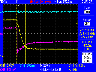
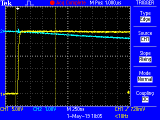
The turn on characteristics when C122 = 0.1uF:

CH1: TP53 - TP10

CH2: TP69 - GND

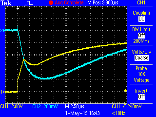
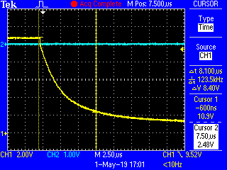
The turn on characteristics when C122 is removed, the voltage dip on TP169 has increased:

CH1: TP53 - TP10

CH2: TP69 - GND

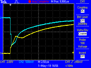
The turn on characteristics when R116 is removed, the Vgs has an acceptable rise time. What is the limitation of that causes this slow turn on to happen when the FETs come into picture? I have also tried increasing C122 to 2.2uF, with no improvement in the turn on time.

CH1: TP53 - TP10

CH2: TP69 - GND


Complaints with Turn-off

A similar issue is observed with the turn off of the FETs. It is seen that the turn off is not rapid. (Tfall < 500 ns). Based on the documentation, it is to be noted that the turn-off time is dependent on the value of R108 and C100. Tuning this value to R=10 ohm, C = 0.01uF does not change the turn off time either.


Because of this, the FETs are not able to sustain a direct short at the battery pack level, and are failing due to SOA breach. Can you provide recommendations to:

1. Reduce tf (Fall time) while turn off

2. Have a cleaner turn off without artifacts (Reduced rise time)


Thanks

  • Hi Rachit,
    Current flows in a loop. At DSG turn on current flows from the VDDCP (TP84) out the DSG pin, through the gate resistance to charge the gate capacitance. Current out the source will return to GND either through the PACK pin filter R108 and C100 or the load on PACK+. Current continues from GND through the supply for BATT+ (and/or C43 etc) through R119 or C122 to the VDDCP capacitor C120. As the FET turns on, current will be drawn from BATT+ to PACK+ depending on its load which will raise PACK+ and may pull down BATT+. So there are a lot of dynamics in the circuit.
    When you remove R116 the current is greatly reduced, DSG rises very quickly as the pin capacitance and that of D36 are quite low. DSG rises quickly as your waveform shows, it is not clear why BAT would be dropping.
    The internal path resistance of the BQ76200 is fixed. You can adjust R119 or C122 to hold up BAT. Larger C122 can make it harder for the part to follow load transients on BATT+. Smaller R119 can allow more current into the part during transients. The best solution for your application may depend on the transients present in your system. Reducing R116 will similarly allow more transients into the part.
    For turn off you have selected FETs with low RDSON, they also have a low VGSTH so it is harder to turn them off. The BQ76200 pulls DSG toward PACK. There are internal resistances and the external resistance of R116 or the drop across D36. See www.ti.com/.../slua794.pdf section 4.3. So there is the voltage drop across DSG to PACK and the drop across D36 for the initial phase and the drop across R108 as PACK+ falls. D36 allows transients into the part of course, a schottky type diode would allow a lower voltage drop during conduction. Smaller C100 or R108 will allow the PACK pin to more closely follow the PACK+, again with the tradeoff of more transient allowed to the part.
    You might look at this recent post e2e.ti.com/.../796073 for external driver ideas, but similar limits in the circuit will control the input of the external driver. Biasing the PACK pin below PACK+ or pulling the gate to GND may be better choices with a very low VGSTH FET, I don't know of a demonstration circuit for those approaches.
  • Hi,

    Thanks for the feedback. Adding an external PNP pull down circuitry helped to lower down the Vgs in < 300 ns. Attaching the waveform below:

    CH1: Vgs

    CH2: BATT

    CH3: Vbe (PNP)

    Pain point 1: There is a residual voltage of 2V that decays with a high time constant (Waveform not added in the post)

    Pain point 2 (Unadressed in previous post): The turn on waveform is still not smooth, and needs to be addressed. Any leads on that?

  • Hi Rachit,
    Point 1. DSG does not drive completely to PACK pin, drive becomes high impedance resistive. Similarly the PNP will turn off and any connection becomes resistive with any value provided. When these are off the external resistor R22 is what brings the gate to 0. R22 must be large and it will take a long time.

    Point 2. "Current flows in a loop. At DSG turn on current flows from the VDDCP (TP84) out the DSG pin, through the gate resistance to charge the gate capacitance. Current out the source will return to GND either through the PACK pin filter R108 and C100 or the load on PACK+. Current continues from GND through the supply for BATT+ (and/or C43 etc) through R119 or C122 to the VDDCP capacitor C120. As the FET turns on, current will be drawn from BATT+ to PACK+ depending on its load which will raise PACK+ and may pull down BATT+. So there are a lot of dynamics in the circuit."
    The current out of DSG must come from C122 and from R119 to make up any current from the capacitor. If you have a fast rise your could have internal losses as DSG rises. If your voltage is sufficiently low you may not. See www.ti.com/.../slua794.pdf figure 11 and related discussion. You will have to find the cause in your application.