This thread has been locked.

If you have a related question, please click the "Ask a related question" button in the top right corner. The newly created question will be automatically linked to this question.

BQ24160: Reverse boost protection

Part Number: BQ24160
Other Parts Discussed in Thread: BQ25890

Hi Sir,

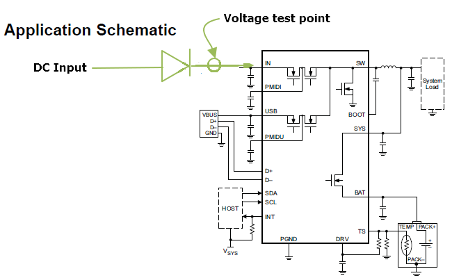
         Regarding to the reverse current protection of Charger BQ24160, we try to add diode to prevent this phenomenon (base on BQ24160 reverse boost issue), as follows,


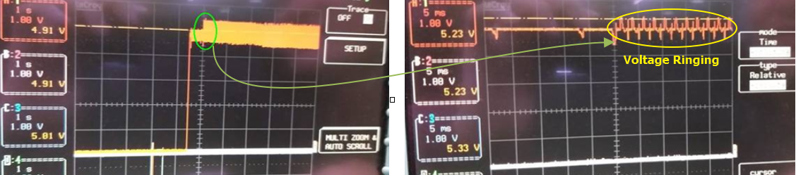
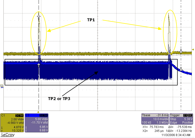
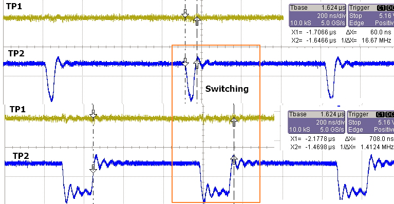
        We found that they have voltage ringing on the Voltage Test Point about the above application, refer to the next figures,

         Figure 1,                                                                                                                                                             Figure 2,


              Could you have any suggestions about this application schematic?

thanks

Jingle


  • Figure 1,                                                                                                                                                               Figure 2.

  • Hi Jingle,

    At what battery voltage does this happen?

    Regards,
    Jeff
  • Hi Jeff,
    Without using the Battery, and we use the QFN package to implement,
    maybe something wrong for this application schematic,
    So, could you please add a diode to EVK to check this issue?

    thanks,
    Jingle
  • Jingle,

    Without a power source at the output (the battery) the IC cannot reverse boost. This IC has forced PWM, which means it does not enter DCM and always has inductor current (even negative) in CCM. So, there will be more ripple than a non-forced PWM buck converter on the input.

    Regards,
    Jeff
  • Hi Jeff,

                From our test, if no battery and no diode, the input voltage (Charger IN) was stable and no voltage ringing, 

                But if no battery and add diode, the input voltage (Charger IN) have voltage ringing,

               Could you explain why use diode is going to have voltage ringing on the input?

    thanks,

    Jingle

  • Hi Jingle,

    Because the charger operates in forced CCM, there is a small amount of reverse current from the inductor that flows back to the input.  The capacitance on the input needs to be large enough to absorb that inductor current.  Without the diode, I suspect that your input source's output capacitance is helping to absorb that current.  Alternatively, you can increase the BQ24160 PMID and/or IN/USB capacitance to prevent the pulsing with diode, but doing so could violate the USB inrush current requirement.

    Regards,

    Jeff

  • Hi Jeff,

               Thanks for your quick reply, we do some testing about that application schematic (No Battery and have diode), as below,

               1. Using AC to USB adapter to supply to our device (Only USB Power, No USB signal), the charger output voltage is stable and our device is working properly

               2. Using DC Power Supply (Model: Tektronix PS280) to supply to device, we found that the charger output voltage isn't stable, we check some pin behavior of the charger, please see the next,

                      A, Test Point figure, TP1 for IN pin, TP2 for Boot pin, TP3 for SW pin,


             B, TP1/TP2/TP3 figure


          C, We add 220uF to the IN pin, the TP1 voltage seems to be smooth(PMIDI is similar to TP1), but the charger output voltage isn't stable, we found the TP2 (SW2) switch in different frequency

                (Working device frequency or PWM/Duty is 708ns stable, not 60ns, and NO switching )


           Base on the above test, the charger seems to do re-boot constantly when the frequency switching, just only add diode into the IN pin,

           The TP1 diode are directional, why to use the diode and DC power supply have to produce incorrect PWM output in the SW PIN?

           I guess it should be dependent and is it possible to have a relationship between the frequency and the internal setting procedure of the charger?

    Jingle

  • Jingle,

    The last plots looks as if the charger is running in max duty cycle mode. Is that plot with both 220uF at TP1 and the diode?  What is the voltage at the IN pin? 

    Regards,

    Jeff

  • Hi Jeff,

                 We add 200uF between diode cathode and IN pin,

                 The input voltage is 5V!

    thanks,

    Jingle

  • JIngle,

    I am not able to reproduce your exact waveform but I see some odd behavior with the diode and additional capacitance on IN. When I enable no battery operation (reg0x01b0=1), which disables reverse boost protection, the odd behavior goes away. It appears that the reverse boost protection circuit is not compatible with the diode and additional capacitance. So, I cannot recommend adding a series diode for this device. With reverse boost protection disabled and the diode, there is a risk of boost back.

    Regards,
    Jeff
  • Hi Jeff,
    1. With reverse boost protection disabled and the diode, there is a risk of boost back.
    => this phenomenon we will keep an eye on when we use it.

    2. We modify our MCU FW and use DC power input, first, the charger has Vsys output stably, MCU will write SDA data (Vdpm=4.6v) to Charger by I2C bus, base on application schematic that we use a diode to do reverse protection, a diode has 0.3~0.4v voltage drop (if use DC=5V), charger IN pin voltage seems to less than Vdpm register setting, the charger will turn off Vsys output, so our MCU is all disable because of no MCU power input, now I think it's a right process,

    About the above description, could you provide the detailed internal voltage comparison structure of charger for our reference,

    thanks,
    Jingle
  • Jingle,

    Can you be more specific about the internal voltage comparison structure to which you are referring?

    Regards,
    Jeff
  • Hi Jeff,

               For example, charger IN pin voltage=4.5, and the charger Vin_dpm setting 4.6V,

               BQ24160 internal how to judge or compare voltage between Vin and Vin_dpm, and decide the SW pin has no output?

               We want to know this procedure of the charger, please tell us.

    thanks,

    Jingle

  • Jingle,

    VINDPM error amplifier is not shown in the BQ24160 block diagram but is shown in the BQ25890 datasheet www.ti.com/.../bq25890.pdf page 17. The amplifier compares the input voltage to the VINDPM setting. As the input voltage drops close to the set point, the error amplifier clamps the PWM duty cycle, which effectively reduces the maximum allowed input current.

    Regards,
    Jeff
  • Hi Jeff,

               It's clear to me now,

               By the way, what is the allowable range of voltage that VIN is close to Vin_dpm? 

               For BQ24160 datasheet, VIN_DPM threshold accuracy: -2%~+2%

               So, VIN_DPM=4.6V, the range is equal to 4.692V, If VIN < 4.692V, the SW output will be closed.

               Is it correct?

    thanks,

    Jingle

  • Jingle,

    Correct.

    Regards,
    Jeff