This thread has been locked.

If you have a related question, please click the "Ask a related question" button in the top right corner. The newly created question will be automatically linked to this question.

UC2715: Driver IC Heating Issue

Part Number: UC2715
Other Parts Discussed in Thread: UC1825

Dear Sir,

I'm using UC2715 Complementary Switch FET Driver with Auxiliary Output, for Forward converter with active clamp. Vcc is 12V  and its switching at 100kHz and the primary main MOSFET is having total Qg of approx 90nC, and Auxilary output is used for active clamp MOSFET thats N-channel driven with pulse transformer. 

  • Primary Driver IC at ambient (25 degree) after keeping for 1Hr @ secondary full load (5V/ 30A) is heating up to 60 degree. what are the possible reasons for this much temperature rise on the IC (SOIC-8 package)
  • Is there higher operating temperature 125 degree available for same package SOIC-8.

Regards,

Nesh

  • Hi Nesh,

    Thanks for your interest in our driver, my name is Mamadou Diallo, I am an AE supporting low-side drivers.

    From your description, with the driver operating at Vcc=12V, fsw=100kHz and a load of 90nC, you should expect a power dissipation from the driver to be at P=2*(12V*100kHz*90nC)=216mW (dual channel worst case) which this device thermal ratings should be more than capable of handling. Under those conditions, you should only be seeing ~19.22DegC in junction temperature rise.

    What does your layout look like? Can you please share your schematic/layout? Does the primary MOSFET heat up as well or just the driver? I ask this because junction temperature rise can be related to many factors including layout. It is also recommended to use an external gate resistor which will help share the dissipated power during the switching transitions.

    Additionally, are there specific features that attracted you to this driver? I ask because I can maybe interest you in one of our latest most optimized driver commonly used in these applications.

      UC2715 UCC27524 UCC27524A
    Datasheet Datasheet Datasheet
    Number of channels (# ) 2 2 2
    Power switch MOSFET MOSFET MOSFET
    IGBT IGBT
    GaNFET GaNFET
    Peak output current (A ) 2 5 5
    Input VCC (Min ) (V ) 7 4.5 4.5
    Input VCC (Max ) (V ) 20 18 18
    Rise time (ns ) 30 7 7
    Fall time (ns ) 25 6 6
    Prop delay (ns ) 50 13 13
    Input threshold TTL CMOS CMOS
    TTL TTL
    Channel input logic N/A Dual Dual
    Non-Inverting Non-Inverting
    Input negative voltage (V ) 0 0 -5
    Features Dead Time Control Enable Pin Enable Pin
    Rating Catalog Catalog Catalog
    Operating temperature range (C ) -40 to 85 -40 to 140 -40 to 140
    Package Group SOIC | 8 MSOP-PowerPAD | 8 MSOP-PowerPAD | 8
    PDIP | 8 SOIC | 8
    SOIC | 8  
    SON | 8  
    Approx. price (US$ ) 1.17 | 1ku 0.65 | 1ku 0.75 | 1ku
  • Dear Sir,

    I'm using external gate resistor 1.5E, MOSFET is heating normally only as per power dissipation. The input PWM signal for driver IC is taken from UC1825.
    I'm interested more with UC2715 is because of the complementary Aux output and dead time control.
    Sir could you please share me the main points to be considered for the layout for driver IC UC2715.
    And also what are the worst case conditions in layout which will lead to heating of driver IC.

    Regards,
    Nesh
  • Hi Nesh,

    Layout can impact the driver in several ways:

    -The first and most obvious is the loop inductance of the peak current in the gate drive portion where the bigger this loop, the higher the stray inductance in the gate drive path which in combination with the di/dt in this same loop will ultimately result in ground bounce in the circuit (from V = L*di/dt where two points on the same node have different voltages) as well as high-frequency oscillations and higher/longer voltage spikes that increase power dissipation and pose a risk of damage to the device. To prevent this, the FET(s) must be placed as close as possible to the driver's output stage to reduce the loop inductance in the peak current path.

    -From your description mentioned that you're using a 1.5-Ohms gate resistance, from the power dissipation formula of our drivers, P ~= 1/2 * Qg * Vcc * ƒsw * [ { 1 / (1 + Rgate) + ( 2 / ( 2 + Rgate) } ]. You will notice that a higher gate resistance will reduce the power dissipated at the junctions of the driver at expense of slower rise/fall times.

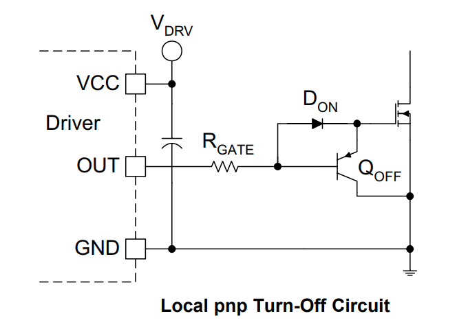
    -You may also further reduce the power dissipated within the driver by using a local pnp turn-off circuit at gate to confine the turn-off current to a small area. This would reduce the total power dissipated by a factor of 2 since the turn-off current never goes back to the driver.

    Please let us know if you have further questions or press the green button if this addresses your question.

    Thanks.

    Regards,

    -Mamadou

  • thanks for the reply sir.
  • Dear Sir,

    what is the thermal resistance of UC2715 SOIC-16 package (K/W)?
    1. Nominal Icc is 24mA (as per datasheet) and the Vcc is 12V in my board, therefore the total power dissipation is minimum of 0.288W.
    2. This power dissipation itself will cause how much temperature rise on the IC.
    3. Is there higher operating temperature 125 degree IC available for same package SOIC-16.

    Regards,
    Nesh
  • Hi Nesh,

    This is an older device therefore thermal resistance for this device is only approximation and not verified.
    Similar technology driver with same package (soic 16) UC3708DW has Θja of 66.9℃/W, you may use this value as estimated value only.

    You're correct that Pdc = Icc * Vcc. This is the power dissipation during standby mode when the device is on but not switching.
    The total power dissipation of the driver has two portions: Pdiss = Pdc (static) + Psw (during switching) = Icc * Vcc + ( 1/2 * Qg * Vcc * Fsw * [ { 1 / ( 1 + Rgate) } + 2 / { 2 + Rgate} ] ). The driver's quiescent power dissipation is rarely a concern as heating and increase power dissipation is related to the driver's Psw.

    Using Pmax = (Tj - Ta) / Rtja
    where Pmax is the maximum allowed power dissipation in the gate driver;
    Tj is the recommended maximum operating junction temperature;
    Ta is the ambient temperature of the gate driver and
    Rtja A is the estimated junction-to-ambient thermal resistance

    Pmax allowed = 1.86846W

    Adding Pdc + Psw = 288mW + 216mW ~= 504mW well below the max.

    I strongly believe there some external factors contributing to this heating.

    We don't currently have dual low-side in soic 16 package available.

    Regards,

    -Mamadou