


I've implemented the TPS61088-Q1 into a design with the following schematic:
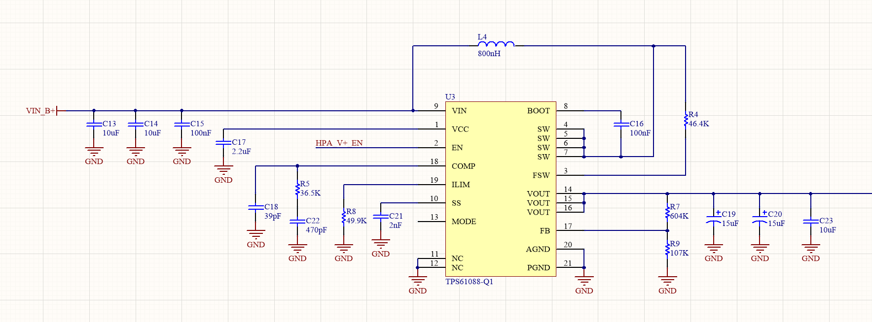
The input is 3-4.2 V and I need to boost up to 8V at 2A. I got this design using the WEBENCH tool.
When I supply the input voltage at 4V, I see 3.5V at Vout, which is expected when the device is not enabled. However, when I supply 3.3V logic at the enable pin, the state does not change at all. Still 3.5V at Vout. I probed both Vcc and the SS pins before and after asserting the enable pin, and strangely both pins read at 0V. I expect the Vcc pin to have some kind of voltage output regardless of enable, but it appears that the internal LDO isn't being enabled to supply the IC. Am I missing something or is there an error in my application?
Thanks,
Markus

