This thread has been locked.

If you have a related question, please click the "Ask a related question" button in the top right corner. The newly created question will be automatically linked to this question.

TPS61322: Overheating

Part Number: TPS61322
Other Parts Discussed in Thread: ADS1299

Hello, 

I have designed the circuit and 2layer PCB below for charging and boosting the output of a LiPo battery from 3.7V to 5V.

I am using the TPS613222ADBVT chip to boost the LiPo output from 3.7V to 5V.

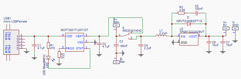
When the switch is set to boost mode (disconnecting charge circuitry), I am getting 5V at the output as expected.

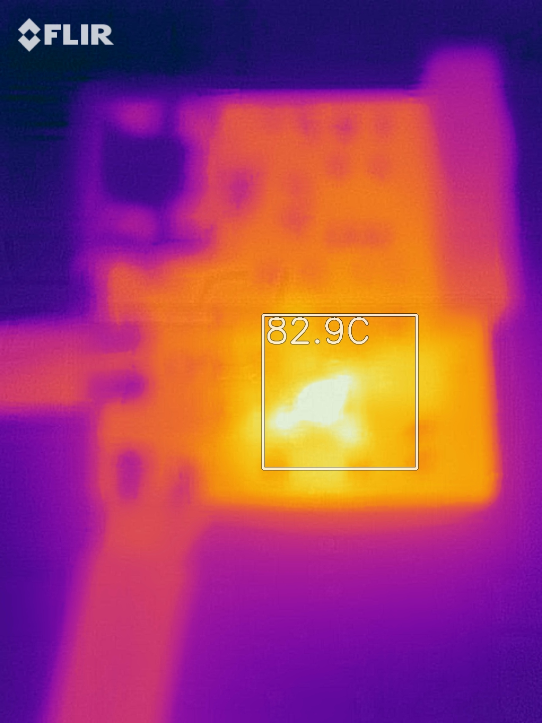
However, the board gets very hot in less than a minute. The inductor in particular gets extremely hot. 

Can someone please tell me if this is normal, or if there is something wrong with my circuit that is causing it?

Is there any method to dissipate some of this heat without enlarging the footprint of the PCB too much?

Would more vias to the ground plane on the bottom layer help?

  • Hi Mark:
    May you able to check which part is the hot source? Is the converter?

    And what's the load condition?
  • Hi Minqui,

    When I put the switch to position 2 (turning on the boost converter circuit), the entire boost circuit heats instantly.
    Just from touching the components, it seems like the convertor and inductor become hottest and very quickly.
    The inductor is a Bourns SRP2512-2R2M (2.2uH, 2.1A current rating, 3A sat current, 104mOhm DC res). Very similar spec to the inductors recommended in the TPS61322 datasheet.
    The capacitors I'm using are all 0603 size and X5R as reccomended in the datasheet.
    The Schottky Diode is the On Semi NRVTS245ESFT1G. Would making the capacitor in the snubber circuit larger make any difference?

    I have tried it with no load, and within seconds the board heats to the point where the converter and surrounding components can't be touched.

    With a 15Ω load, I have checked and the current draw is 0.33A as expected (5V/15Ω). The load resistor heats excessively to the point where there is a burning smell, but that's expected I suppose with over 1.6W running through it. 

    The converter and surrounding components heat up with or without a load.

    Could it be related to the answer here which suggests that a diode with too slow reverse recovery time could cause additional heating?

    Or if this heat generation is expected, is there any easy way to sink some of the heat without adding majorly to the size of the board?


    Thank you for your help.

    Mark

  • Hi Mark:
    Sorry that I just back office today.
    It would be hot even with no load? Please just remove the diode and snubber circuit, and re-test with no load. If the circuit is still hot, please catch the waveforms about the Vin, Vout, SW, and measure the input current. If not hot anymore, we could assume the issue is around the external diode, and snubber circuit. We could do the deeper analysis after the test.
  • Hi Minqui,

    I got a thermal camera to look at the board look accurately. Turns out its the snubber circuit causing the heating. In particular the 5Ohm Resistor I think.

    With the R = 5Ohm and C = 100pF values (which are suggested in the datasheet), the temperature rises above 80degrees as seen below.

    I swapped those out for R = 470Ohm and C = 2.2uF (just because I had those values lying around). The board stayed below 25 degrees and I got a clean 5V output.

    I also tried removing the R and C, just leaving the Diode. And there was no heating issue. The board stayed below 25 degrees and I got a clean 5V output.

    I also tried removing the R, C and diode. The board stayed below 25 degrees and I got a clean 5V output.

    Can you please tell me which situation is best? As from what I saw, all gave similar results.

    With the diode and snubber circuit, the output is slightly lower (4.97V). Without it, the output is slightly higher (5.02V).

    As I need a very small footprint, I would prefer less components. So if the output is a clean 5V and there's no heating issues, why shouldn't I just remove the Diode and Snubber circuit?

    Would this put the board at very high risk for large voltage spikes, or would the capacitors to ground minimise this?

    Thanks,

    Mark

  • HI Mark:
    For the snubber, we have a application note about it. It may help you to understand it better.
    www.ti.com/.../slva255.pdf

    For TPS61322, what's your load condition? If the load is light, then you could remove the snubber and the diode.
  • Hi Minqiu,

    The 5V output is powering a TI ADS1299 chip.

    It's does not draw that much current. Do you think it would be ok to remove the snubber and diode?

    Thanks,

    Mark

  • HI Mark:
    It's ok to remove them, just take care about the thermal solution.

    The purpose why we recommended adding the diode and sunnber is mainly for the large load with high Vout.