This thread has been locked.

If you have a related question, please click the "Ask a related question" button in the top right corner. The newly created question will be automatically linked to this question.

TPS65150-Q1: Schematic check

Part Number: TPS65150-Q1

Hi, Team:

Can you help to check attached schematic and advise if any questions?

Just reminder: The  
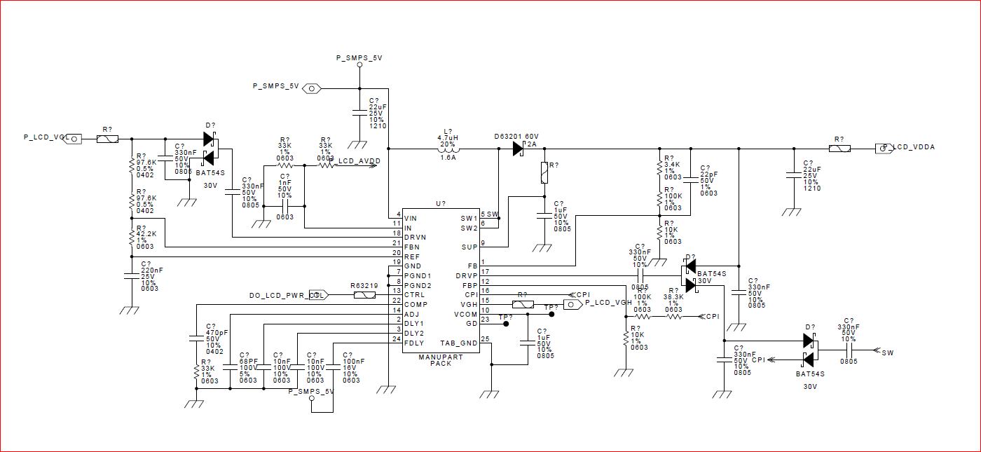
Feedback resistor value is very low compare with datasheet suggestion. 

  • Hi,

    I have notified our expert regarding this topic. Please expect a response by 5/15/19.

    Thanks,
    Aaron
  • Hello Alpha,

    I reviewed this schematics and have following comments. The schematics is not annotated so it is hard to describe changes without referring to actual reference designators but I will try.

    - Since this is VIN=5V application, datasheet recommendation for compensation components is Ccomp=2.2nF and Rcomp=0 ohm. Current schematics is using 470pF and 33K.
    - With the resistor dividers shown in the schematics, I calculated the LCD_VDDA to be ~13V and VGH to be ~18V. With these voltages for LCD_VDDA and VGH, positive charge pump should be used in doubler mode and not the trippler mode that is shown in the schematics right now. So second stage of positive charge pump can be removed.
    - With feedback resistor values shown for boost converter, feedback forward capacitor should be a much higher value (~147pF) instead of the current 22pF shown. Please use datasheet equation 20 and datasheet table 2 to calculate appropriate value for this capacitor.

    Kind Regards,
    Liaqat
  • Hi, Liaqat:

    Thanks for the update.

    What about the feedback resistor value? No issues, right? 

  • Hi Alpha,
    Although these smaller values will have higher leakage current but they should be ok otherwise.
    Kind Regards,
    Liaqat