


Dear support member,
My customer used TPS22990.
I have a question.
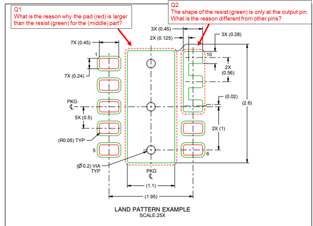
(Question1)
What is the reason why the pad (red) is larger than the resist (green) for the (middle) part?
(Question2)
The shape of the resist (green) is only at the output pin.
What is the reason different from other pins?
Best regard.
Bob Lee.

