This thread has been locked.

If you have a related question, please click the "Ask a related question" button in the top right corner. The newly created question will be automatically linked to this question.

AC-DC power supply mosfet mounting clarification

Hi There,

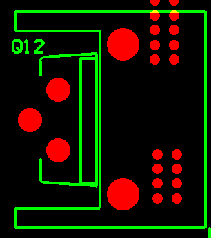
I could see many power supply design from TI having mosfet in this kind of orientation (image attached below). I hope this is for better clearance routing. My Question is if it going for production how they will solder this thing in the fast manner. Whether any factory custom available for the kind of solution or this need be done from our side like manual soldering. Please advise 

  • Hello Balasubramani,

    The center leg of high-voltage transistors is usually extended from the other two legs in order meet safety agency creepage and clearance requirements at the pcb level. Commercial PSU designs are subject to the same world-wide requirements and they also extend the center legs in a similar manner.

    Whether the transistor is mounted stand-up (as shown) or lay-down (for low board height), the PSU manufacturer is responsible for cost-effective assembly of these parts. They can purchase the transistors in standard form and bend the legs at the factory, or purchase them pre-formed if the volume is high enough. Their manufacturing engineering will design high-volume assembly fixtures to hold these and other large components in place for wave-soldering or reflow soldering, depending on their process. Low volume assembly and soldering is typically done manually.

    Since most manufacturers have different and unique assembly processes, the exact fixturing and process flow will be different from one vendor to another. They may be similar in concept but differ in details, so each manufacturer will have a custom solution for preparing and soldering these heat-sinked transistors to their boards.

    Regards,
    Ulrich