This thread has been locked.

If you have a related question, please click the "Ask a related question" button in the top right corner. The newly created question will be automatically linked to this question.

WEBENCH® Tools/UCC28634: The UCC28634 does not provide initial pulses and a MOSFET damage.

Part Number: UCC28634
Other Parts Discussed in Thread: UCC28630EVM-572

Tool/software: WEBENCH® Design Tools

Hello,


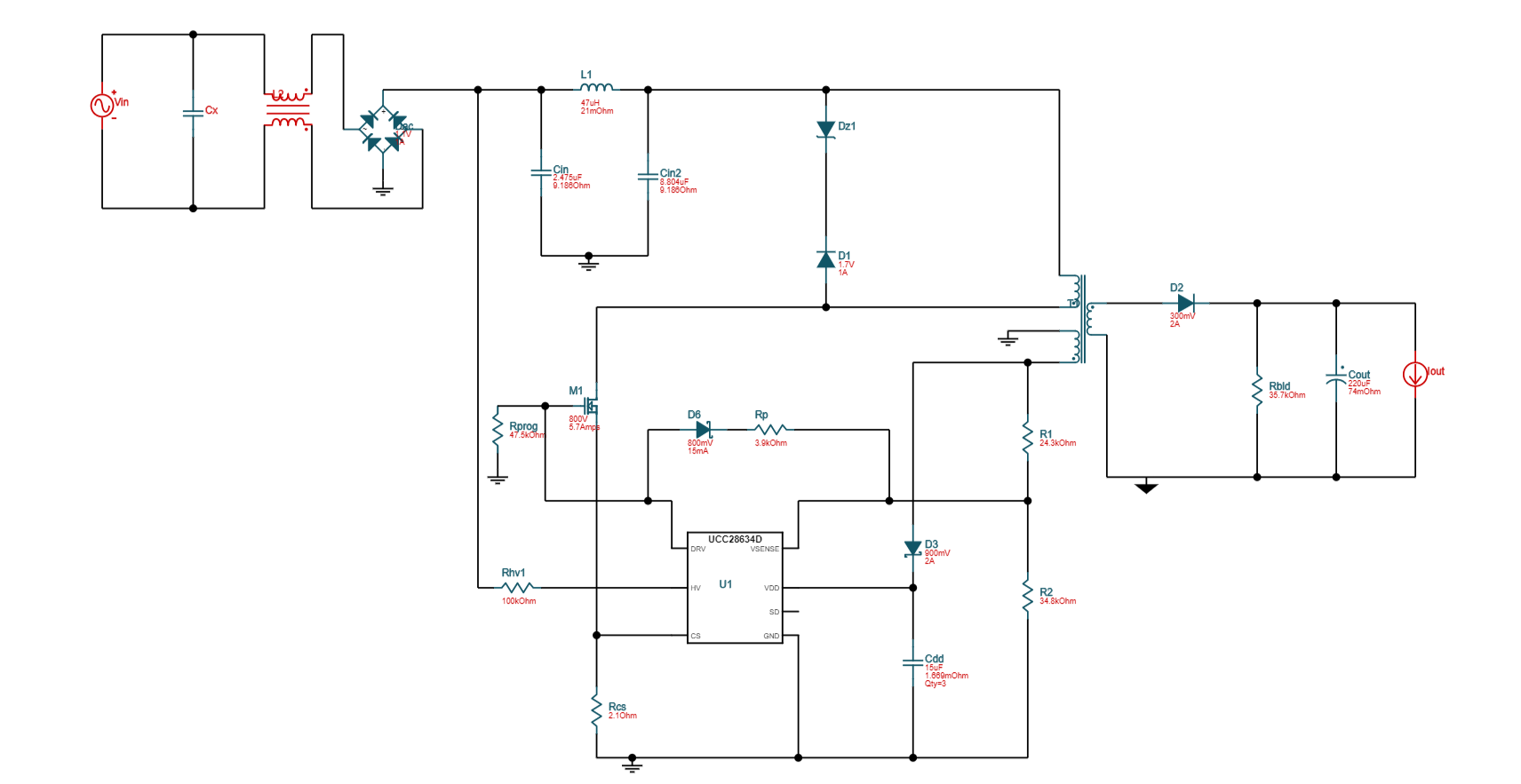
We are currently using UCC28634DR flyback controller for a closed-loop control in a flyback project (Vin = 240VAC, Vo = 12VDC, Io = 0.5A). We are using the Webench design shown below. All the components we purchased are the recommended in the diagram except for the transformer which we hand-made (ratio = 1:7 for both secondary and auxiliary).

The project works successfully as an open-loop when we provide the switch pulses from a microcontroller and the outputs in both the secondary and auxiliary sides are 12VDC. The off-state voltage spike is only 465V. This open-loop test indicated that the transformer and the switch were working properly. However, every time we run the circuit using the UCC28634D with the configuration below, the switch (600V,16A MOSFET) gets damaged (shorted). We even used a snubber circuit (R= 4.7K, C = 10nF) in addition to the recommended clamp diodes and the mosfet still gets damaged.


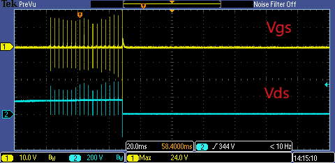
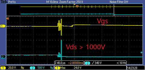
We debugged the circuit using DC input (330VDC) instead of the mains. We saw that when the HV pin in the UCC28634DR is above 40VDC, there are weak pulses established in the mosfet gate but VDD is still 0V. Once we slowly increase the input voltage to 200VDC, the mosfet gets damaged with huge Vds spike (above 800V).


We believe that UCC28634DR to some reason, is not providing the initial pulses to the switch the MOSFET in order to create the auxiliary output to start the functionality.


We would appreciate a help if the configuration below is applicable to our project or not. And why the mosfet is failing at higher HV input than 200V.


Thank you

  • Ahmad

    As soon as the voltage on VDD exceeds VDD(start), which is 14.75V typical, UCC28634 will attempt to start by turning the FET on. If there is no fault (as shown on Table 3 in page 42 of the datasheet) it will power up, otherwise it will go into fault shutdown. Rather than increase the voltage until it fails we recommend that you probe around the IC to understand why it is not starting up.

    Webench is not a comprehensive design tool. While it is great at getting an initial design, engineering due diligence is needed to finalize a design. For parameters such as the snubber, the exact value depends on non-ideal parameters such as leakage inductance, so it's recommended to modify your design to meet the actual component values that you have. If the FET is failing due to overvoltage when the converter is operating in a condition it was designed for, then the snubber is not strong enough. We recommend reducing the voltage of the zener diode clamp or increase the capacitor in parallel with the zener diode to reduce the overshoot.

    It's recommended that you verify that the layout follows the recommendations in section 11 (page 74) of the datasheet and that you use the excel design calculator to verify that all the proper components are used www.ti.com/.../sluc537

    Best Regards,
    Eric
  • Hello Eric, 

    Thank you for your response. 

    The snubber circuit we added was working just fine in the open-loop test. We believe that UCC28634 is not providing the initial pulses to the switch in order to produce voltage in the auxiliary winding of the transformer to perform the feedback to VDD pin (we are getting 0V at VDD pin). 

    Please check Figure 1 below which shows the waveforms we obtained when we tested the schematic above through a DC input and we slowly increased the HV pin voltage. The yellow waveform is the gate pulse (Vgs) and the blue waveform is the drain source voltage (Vds). We notice that there were some initial spikes (some of them were negative?) in the switch just when the voltage increased to  200 V. thereafter, we observe a huge spike across the FET resulting in total MOSFET failure.This happens every time.  

    After zooming the waveform carefully (shown in Figure 2), we noticed the Vgs gate pulse (spike) generated from the IC UCC28634 was distorted too. This corresponds to the huge spike in Vds (above 1000V) which also goes to negative. Could you please explain why we are getting such behaviour ?


    Figure 1


    Figure 2


    Thank you

  • Ahmad

    Before debugging further please confirm that you are following layout recommendations for UCC28634. As section section 11 (page 74) of the datasheet explains, it is critical to have a good layout to insure proper operation. If you do not follow these recommendations then parasitic inductance or capacitance can cause improper behavior, such as excessive ringing.

    If there is never a voltage on VDD UCC28634 will never startup. The way UCC28634 starts up is that there is a internal JFET in the HV pin that acts as a current source to charge VDD. If you never have a voltage on VDD then something is not correct with this circuit. I recommend you read section 8.3.1 (page 15) of the datasheet and confirm that your circuit is operating as expected during startup.

    That being said, it appears that VGS does turn on in Figure 2 you provided in the middle of the screen (DRV gets it's voltage from VDD), so it may actually have a voltage on VDD. It's hard to read the magnitude since it's at 20V/div, but it looks like it could be high enough to possibly turn on a high voltage FET. I recommend that you measure this exact voltage change and compare it to the threshold voltage of the FET you are using to confirm if this is the case or not.

    Once you verify that the layout is correct and the startup circuit is behaving properly I recommend that you review how the VSENSE pin measures the output voltage and the fault conditions it measures. This begins in section 8.3.4 (page 23) of the datasheet.

    If you are still having issues I recommend that you order the UCC2863x EVM UCC28630EVM-572 to have a board to compare what a known good unit behavior is like.

    Best Regards,
    Eric
  • Hello Eric

    Thank you for your response. 

    We did a DC test on the design above at 200VDC input and we found that VDD pin does behave in similar fashion to Figure 16 in the UCC28634 datasheet (see Figure 3 below). The energy storage (bias capacitance) used in VDD pin was initially 90uF. The maximum value of VDD shown in Figure 3 reaches only 14.4V and 4.4V minimum (which means it oscillates above and below the VDD(stop) threshold?). We tried to measure the VGs in the meantime but there was no pulse and the mosfet Vds was not switching.

    We tried to increase the energy storage by increasing the bias capacitance to 217uF but the waveform behaved in similar way with the same peak and trough values of VDD (see Figure 4). We then tried to increase the input voltage to 300VDC and the max and min VDD are still 14.4V and 4.4V respectively.  We are wondering if we have to change our transformers turns ratio ?  Also,  we are wondering if the UCC28634 HV pin should not see a DC input and whether it must be tested using an AC input instead?

    Figure 3: Vdd pin at 200VDC input and 90uF bias capacitance.

    FIgure 4: Vdd pin at 200VDC input and 217uF bias capacitance.

    Regards

    Ahmad Esmaeel

  • Ahmad 

    I assume that the yellow trace in your images is VDD?  Please confirm that no fault condition is active during startup. You could be having a fault condition that is preventing the controller from starting up.

    Table 3 (page 42) of the datasheet has details on which faults UCC28634 measures for.  All of the fault responses for UCC28634 are auto-restart, so when the controller senses a fault event it disables operation and discharges the VDD pin to the VDD(reset) level, followed by a restart attempt.  I recommend that you review all the fault conditions and measure to see if any of them are being activated.

    Best Regards,

    Eric