This thread has been locked.

If you have a related question, please click the "Ask a related question" button in the top right corner. The newly created question will be automatically linked to this question.

TPS54360: TPS54360 Production damage problem

Part Number: TPS54360
Other Parts Discussed in Thread: LMR14030,

Hi Ti team,   

1. Phenomenon: TPS54360 is burnt out in the aging process(Vin=30V,Vout=5V/0.2A-2A) and abnormal impedance was found in Vin, Sw or EN pin

The Vin pin in particular has burned off. About 5pcs out of 100pcs were burnt out

2. Check and test found two problems:

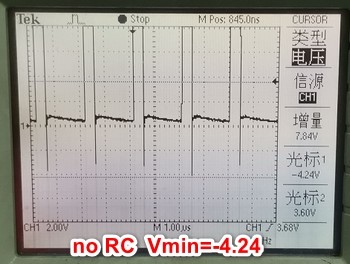
A, IC BucK circuit is not stable, and the waveform of Sw foot is different in size (as shown below)
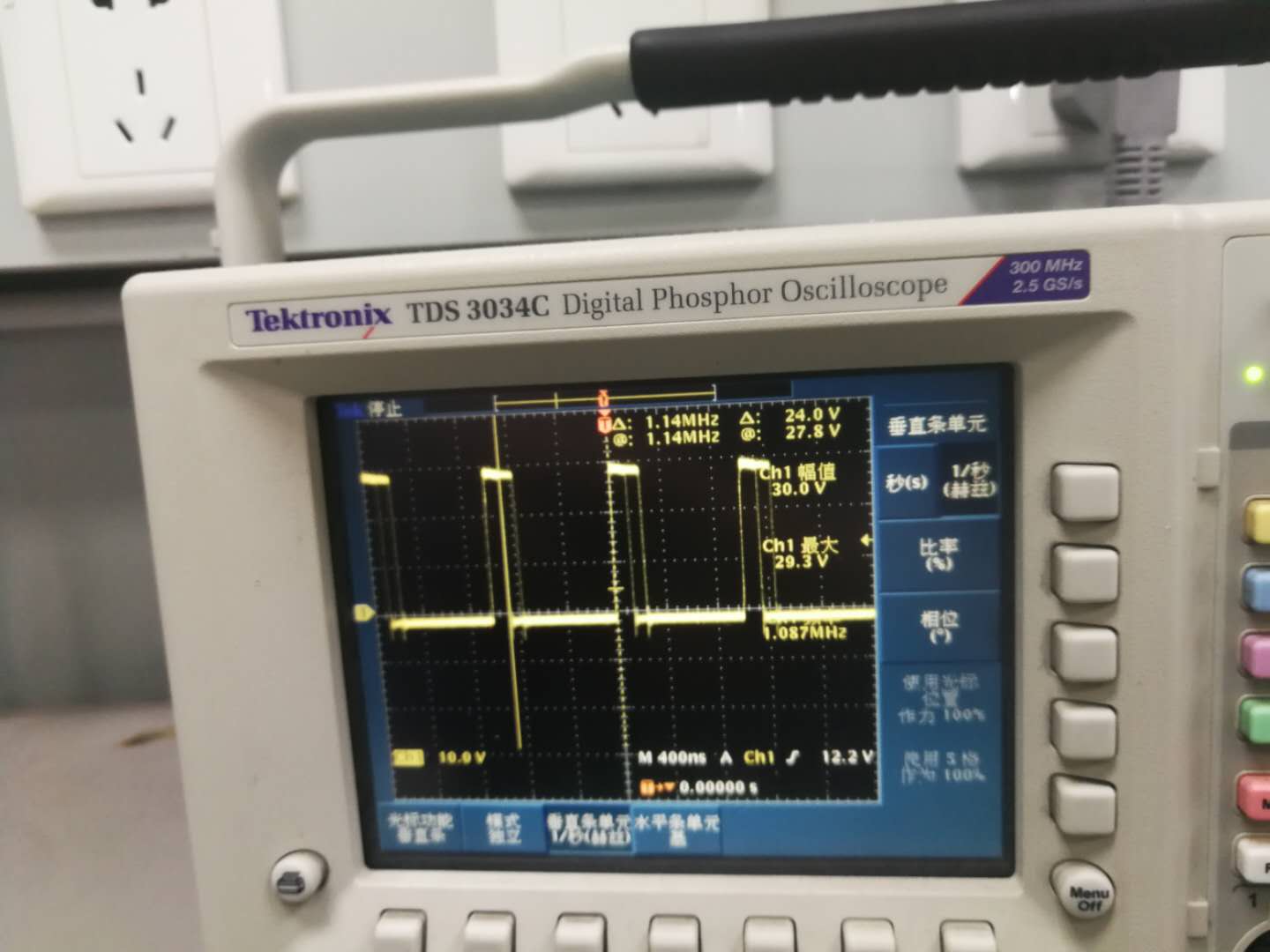
 .

B. Input 30V  start up, Vout 5V/ 1.5a or above current test start up waveform, Vout overshoot up to 8.3v

3. Rectification results:

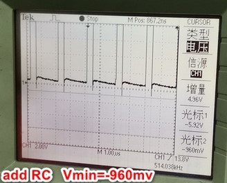
A, FB feedback the capacitance in parallel on the pull-up resistor, C95 0.1uf is removed, and the problem of abnormal waveform of SW foot is improved( test waveform as below)

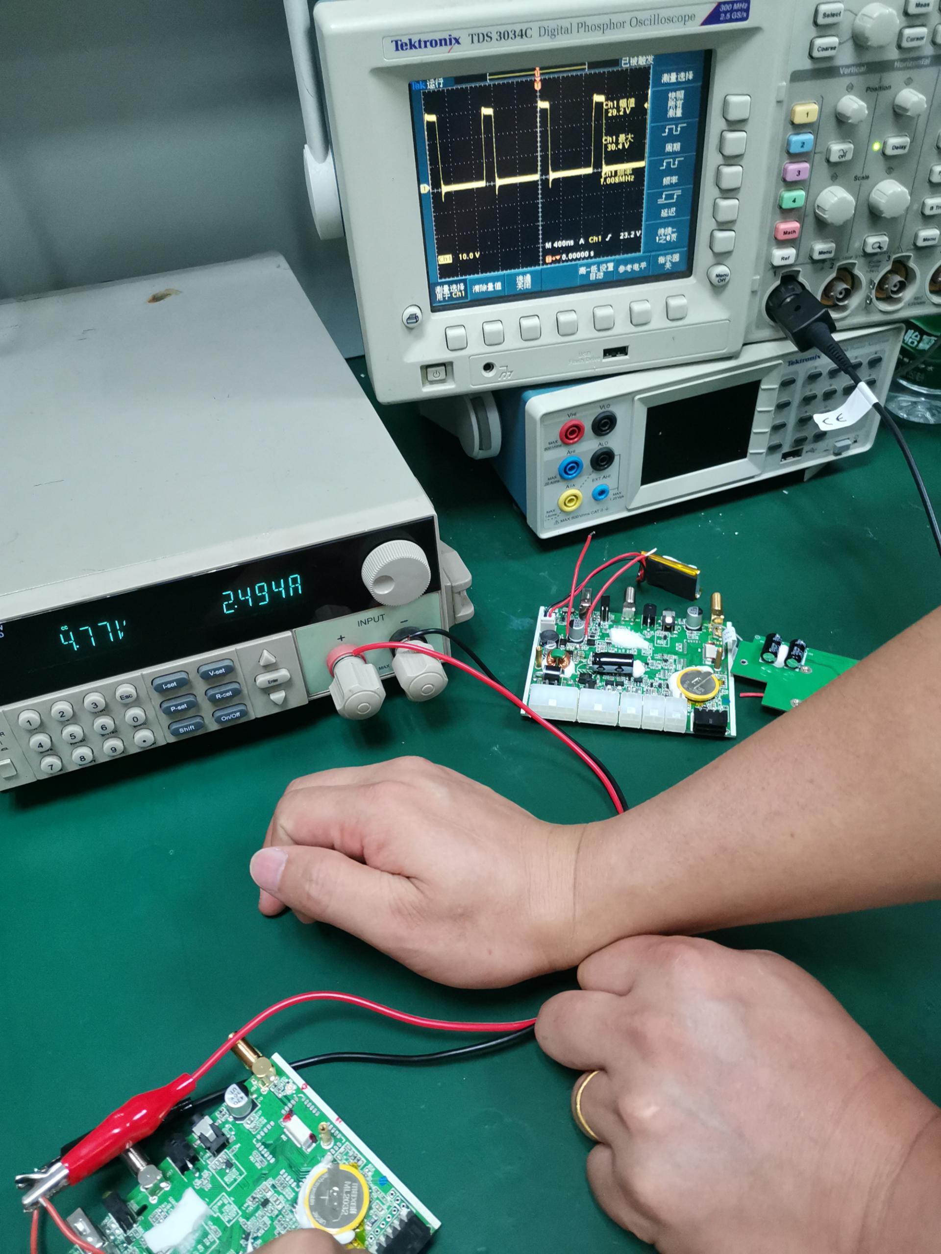
B. The working frequency of the switch is changed from 1Mhz to about 700K, which improves the overshooting problem of output voltage

4, After modification, Producted 100PCS for aging experiments(Vin=30V,Vout=5V/0.2A-2A), and now another one is found burnt out, the phenomenon is the same as before

5,Please help to confirm whether there may be other problems causing such burning?
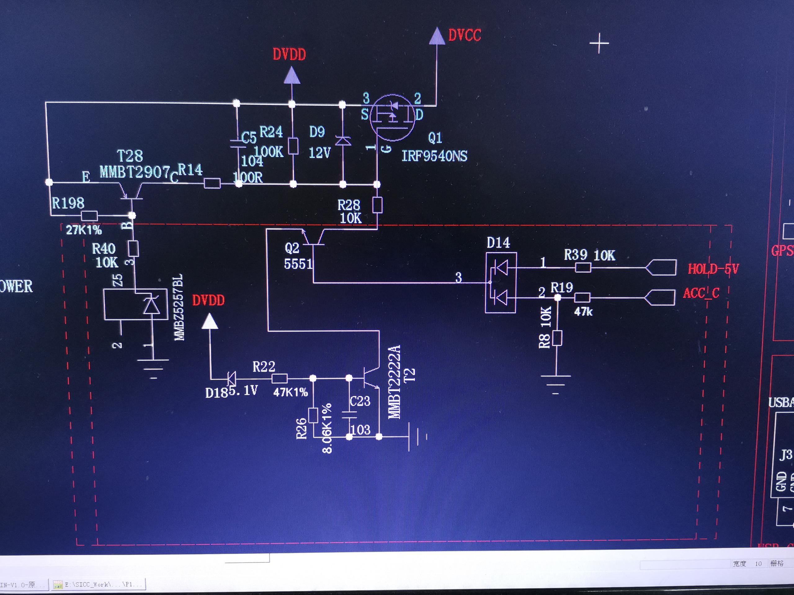
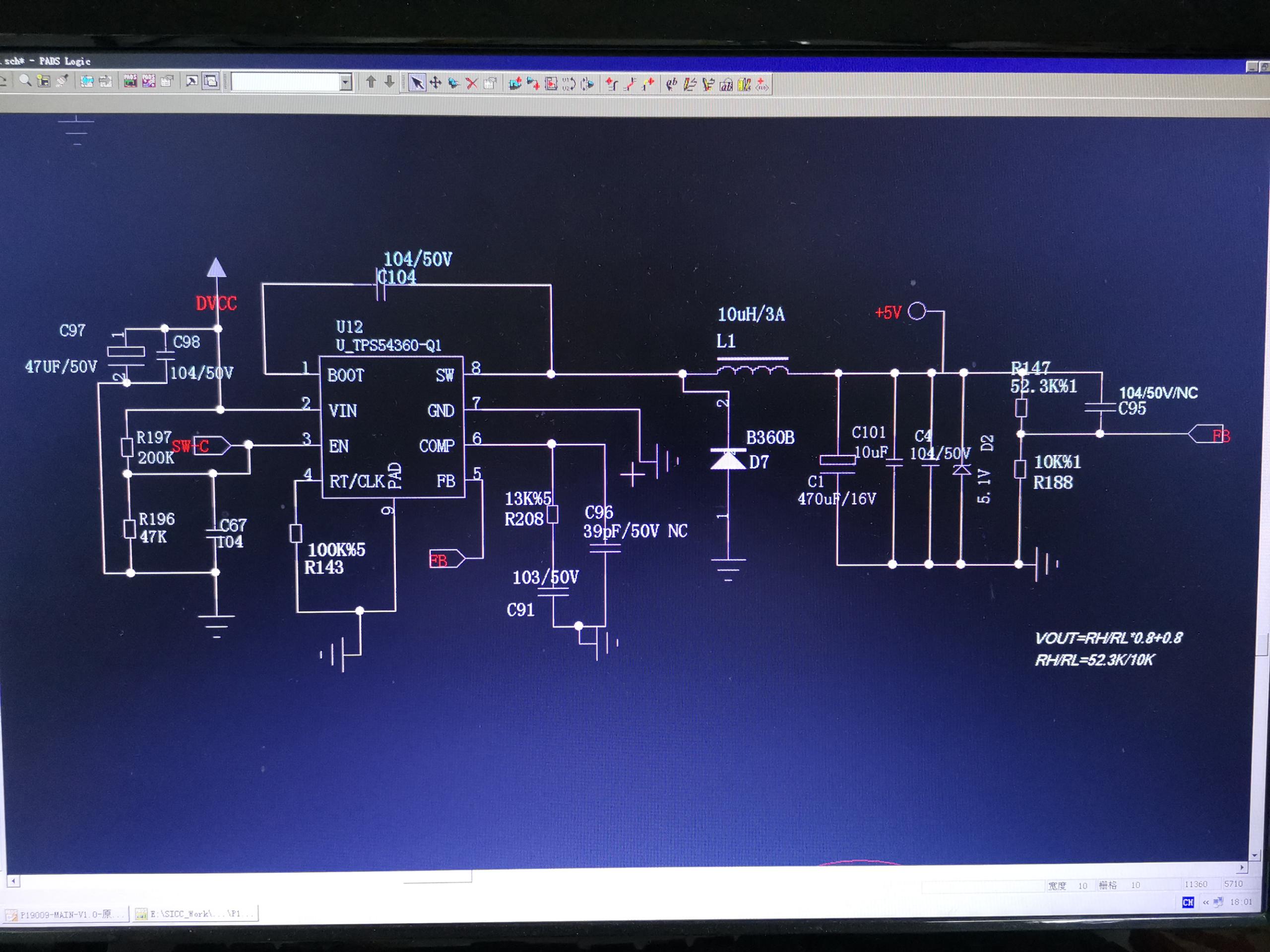
6, SCH as below

  • Hello Jimmy,

    I would check the following:

    1) Does the input of the part overshoot significantly when applying power? The common mode choke will have leakage inductance which may cause input voltage overshoot.
    2) In your oscillograms, it looks like the switch node undershoots below the IC’s Abs MAX rating for this pin. Depending upon which company’s B360B you are using, this may be minimized by diode selection. Layout may also affect this.
    Also, use of the TPS54360B series or, if your maximum input voltage is less than 42 V, the LMR14030 series may drastically reduce susceptibility to this type of noise.
    3) SW-C in your schematic appears to come from off sheet. What is the maximum voltage that can appear on this node?
    Removal of the CFF, C95, is a good idea. Its value depends on the characteristics of C1. I can help with stability if you send the manufacturer’s part number for C1.

    Since this discussion will almost certainly involve confidential information from you side and a detailed investigation and design review may be called for, I recommend continuing by email. Please send me an email at robert.blattner@ti.com.

    Regards, Robert
  • Robert,

         Thanks for your support, I have send the email to you.


    1, SW-C no connect others ,only pull up resistor to VIN and pull down resistor  to GND


    2, C95 is NC

    3, the C1 and D7 datasheet as email to you


    4, Test Vin,EN and SW waveform no find voltage overshoot. Waveform as Email to you

    5,  Help us to see whether  there are any other possible causes of such damage? Thanks!


    Vin=30V, Start up test, In Room temperature


    CH1:SW

    CH2:EN

    CH3:Vin   Vout=5V/0.1A

    CH1:SW

    CH2:EN

    CH3:Vin   Vout=5V/0.5A

    CH1:SW

    CH2:EN

    CH3:Vin   Vout=5V/1A

    CH1:SW

    CH2:EN

    CH3:Vin   Vout=5V/2.5A

  • Robert,

    Could you give us some advise?thanks!
  • Hello Jimmy,

    I am sending an email today.

    Regards, Robert
  • Hello Jimmy,

    Since we have been using email to work on this problem, I am closing this thread.  We can open a new E2E if current solutions do not address your concerns.

    Regards, Robert

  • Robert,   

          Could you please help to confirm whether there are other possibilities causing IC burn out?

    After four times of changing the machine, on June 12, a power IC TPS54360DDAR burned out again in the 100 equipment of the new changing machine

     1,Changed 1: remove capacitor C95;

    At that time, we found the phenomenon of large and small waves  in SW pin and made adjustment


    2,Changed 2: reduce switch frequency to 500KHz;

    Switch frequency is reduced from 1MHz to 500KHz to improve the problem of transient Vout overshooting when starting up and power up. At the same time, large switch frequency causes large losses of circuit components, so this adjustment is made.


    3,Changed 3: add RC absorption circuit to absorb the shock wave at the foot of SW tube.(R=5R,C=4.7nF)

    The original TI factory pointed out in the email that the waveform on SW pin has abnormal undershoot, and suggested that we try the diode on EVM plate.After replacing the diode, the situation was not significantly improved. According to our experience, we added RC absorption circuit and observed the waveform change of SW.After adjusting the parameters of the resistance capacitance, the waveform of downrush is adjusted to a safe range.The figure below shows the comparison of SW waveforms before and after adding RC.

  • Hello Jimmy,

    We have covered the most common problems so I am looping in another engineer who also works with this part. Also, would it be possible to have a board shipped here?  Sometimes, working in the lab is the best way to find problems. 

    Regards, Robert

  • Hello Jimmy,

    Since we have been working using emails, I am closing this thread.

    Regards, Robert