This thread has been locked.

If you have a related question, please click the "Ask a related question" button in the top right corner. The newly created question will be automatically linked to this question.

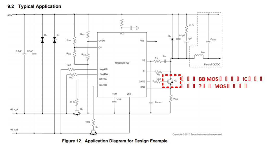
TPS23525: TPS23525 MOS Short Circuit and EN function

Part Number: TPS23525
Other Parts Discussed in Thread: LM5051, TPS23521, LM5069

Dear Team,

1.How to implement ENABLE function with this device?

2.What will the circuit response if the Q1 short circuit?

BR

Kevin

  • Hi Kevin,

    1. Please connect a NPN transistor between UVEN and VEE to implement ENABLE function
    2. if Q1 fails in short, there will not be any control on the power path. So, we will lose power path protection.

    Best Regards,
    Rakesh
  • Hi, Team

    I am doing the project for Delta telecom special application and i think the TPS23525 will be a good solution to be used.

    but i need to know what happend if the IC  fail.

    I list some question about this condition.

     if Q1 short , how to protect?

    according to my experience on this application , the MOSFET is G-D-S short when it damage...

    then it will crush down the gate-driver source and lead to drive source of Q2, Q3 off.  then, Q2, Q3 wiil be heat due to full load.

    how to prevent ? 

    Besids , i saw the PGB function , how does it work?           

    please help me to answer it

    thank you.

  • Hi Wang,

    Welcome to E2E!
    I understood your problem of failing IC (due to Q1 short) can subsequently lead to Q2, Q3 MOSFETs to fail.

    One way to overcome such situation is to use separate controllers for hot-swap and ORing function. For example, TPS23521 for Hot-swap and LM5051 for ORing. I would like to know under which conditions you expect Q1 MOSFET to fail. If we take care in design phase, Q1 fail can be avoided.

    PGb signal is to enable the load only after powering up the system. This is to reduce power stress on the Hot-swap MOSFET Q1 during startup. The PG signal inside TPS2352x device pulls low after powerup, which turns-ON the NPN transistor (refer Figure 14 in TPS23525 datasheet) which pulls up the EN pin voltage of the downstream DC/DC load.

    Please let me know if you have any more questions.

    Best Regards,
    Rakesh
  • Hi, Rakesh

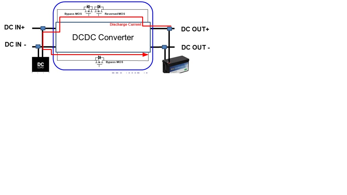
    i know your concern , and our application is not used in output oring function. i want to use TPS23525 appply to  bypass function showed as below.

    Bypass function are composed by Bypass MOS and Reverse MOS. 

    i think thsi IC has a solution to deal with start up in battery discharge.

    DC Out(battery) is source and DC input(RRH). As DC battery charges the Cap of RRH , it must has a great current due to dv/dt  and without any resistance.

    the problem is RRH start up current, i don't know the RRH allowed how much load can endure at start.

    second , if reverse mos damage and lead to Bypass mos 's driver fail . it is very dangerours , it's not controllable.

    Do you have any ideal about this application?

  • Hi Wang,

    TPS2352x is low side controller. So, it cannot function to bypass the positive rail DC OUT+ to DC IN+.
    I suggest to use LM5069 (high side controller) with back-to-back connected MOSFETs as shown in app note www.ti.com/.../snva683.pdf
    The dv/dt control of LM5069 helps to limit inrush currents.

    May I know the reason to bypass the DCDC Converter ?


    Best Regards,
    Rakesh
  • Hi Wang,

    Did you get chance to look at LM5069 device ? Let me know if you have any further queries.


    Best Regards,
    Rakesh
  • hi, Rakesh

    i have took at LM5069 device. although it's a high driver , I have some questions about it.

    1. how to supply VDD?

       The source of MOSFET isn't same grounding at V-battery. 


      if any ideal please let me know

  • hi, Rekesh

    i have took at LM5069 device. I had a question about Vdd

    due to our application , the MOS driver's gound is not the same as the V-battery.

    how to supply the Vdd? anotehr isolated source or V-battery?

  • Hi Wang,

    The internal circuit of LM5069 device draws power from VIN pin, which can be connected to DC IN+. The LM5069 device ground can be connected to DC IN-.
    VDD is pull-up source to pull-up the 'Power Good' PGD pin. The PGD pin can be left OPEN in your application.

    Best Regards,
    Rakesh
  • Hi Wang,

    I hope the above answers your question on LM5069. Please continue posting if you have further questions.


    Best Regards,
    Rakesh

  • Hi, Rakesh

    Actually

  • Hi, Rakesh

    thank you,

    Actually, my application is not like as  bypass function....but I can't pass more information on this.(it's under process.)

    if the different gorund ,does it normally work?

    thank you.

  • Hi Wang,

    I have sent you private message to get more information on your system. Unfortunately, from the above description I did not get clear picture. Please respond privately.

    Best Regards,
    Rakesh

  • Hi Wang,

    We can have a call to close this issue at the earliest. Please check with Kuan Wei Chen to arrange a telephonic call.


    Best Regards,
    Rakesh

  • Hi Wang,
    Please let me know what support is needed to close this ?

    Best Regards,
    Rakesh

  • Hi, Rakesh

    Accroding to our internal discussion, we decided to chose Mechinal short / long Pin to solve the inrush current....

    however, we choose Si8271 to be B&B mosfet driver and ZXGD3112N to Oring control.

    maybe you can introduce the P2P IC to us..

    i'm appreciated your help

    thank you.

    Mechincal

  • Dear All,

    I will close the thread and suggest the solution to the engineer.

    BR

    Kevin