This thread has been locked.

If you have a related question, please click the "Ask a related question" button in the top right corner. The newly created question will be automatically linked to this question.

LM5066: LM5066 issue help

Part Number: LM5066

Hi sir

we use LM5066 meet above questions need your help to check it and give same suggestions,tks!

(1) When each flag bit of all registers is 1, is it valid?
(2) MFR_SPECIFIC_17: BIT14 of READ_DIAGNOSTIC_WORD (E1h) Is IIN_OP_WARN a warning flag indicating current or power?
(3) Write the current of 0.3V to the MFR_SPECIFIC_03:MFR_IN_OC_WARN_LIMIT(E1h) of lm5066 through I2C, and load the voltage of 0.4V to the subsequent circuit of the MOSFET through the electronic load, that is, trigger the input voltage overcurrent warning. Why can I read VIN_UV_fault at 0x78, 0x7C, 0xE1?
(4) The dv/dt output control circuit is only required when starting with dv/dt, but after removing this part of the circuit, OUT is 0 and the MOSFET is not working.
(5) When the dv/dt output control circuit is connected, does the time measured by the TIMER pin include the time of this part? If so, how to determine the time of TIMER?

  • Hi Darren Yang,

    Thanks for reaching out.

    Did you built board with LM5066 ? or Are you testing on TI-EVM ? If you made your own design, can you please share schematic and filled up design calculator. The design tool is available at www.ti.com/.../toolssoftware

    (1) When each flag bit of all registers is 1, is it valid?
    A) It is not expected to observe all the bit to be 1. Did you observed under any test case ?

    (2) MFR_SPECIFIC_17: BIT14 of READ_DIAGNOSTIC_WORD (E1h) Is IIN_OP_WARN a warning flag indicating current or power?
    A) This is the input current warning alert

    (3) Write the current of 0.3V to the MFR_SPECIFIC_03:MFR_IN_OC_WARN_LIMIT(E1h) of lm5066 through I2C, and load the voltage of 0.4V to the subsequent circuit of the MOSFET through the electronic load, that is, trigger the input voltage overcurrent warning. Why can I read VIN_UV_fault at 0x78, 0x7C, 0xE1?
    A)

    (4) The dv/dt output control circuit is only required when starting with dv/dt, but after removing this part of the circuit, OUT is 0 and the MOSFET is not working.
    A) How much is the load capacitance.? Can you send me filled up design tool.

    (5) When the dv/dt output control circuit is connected, does the time measured by the TIMER pin include the time of this part? If so, how to determine the time of TIMER?
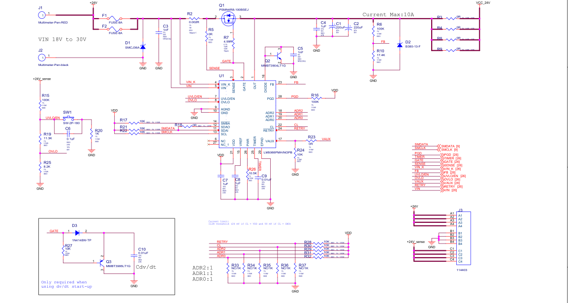
    A) If the device dv/dt rate is set high, the device can enter into power limit mode which makes TIMER to start. Please verify the design using design tool.

    Best Regards,
    Rakesh
  • Hi Darren Yang,

    Can you share your design details as requested above to answer #4, #5 questions.

    Best Regards,
    Rakesh
  • Hi Rakesh

    the SCH is as attachment and we also have two questions need you help to check it and give same way for us,tks!

    1. What is the data of registers 0x78, 0x79, 0x7A, 0x7C, 0x7D, 0x80, 0xE1 after lm5066 is powered up normally (please be expressed in binary)

    2.The supply voltage is 24V. After all the flag bits are cleared, the current of 0.3A is written to the MFR_SPECIFIC_03:MFR_IN_OC_WARN_LIMIT(E1h) of the lm5066 through I2C, and the current of the MOSFET is loaded with 0.4A through the electronic load, which triggers the input current. Overcurrent warning. Use i2c to read 0x78 data as: 00001001; read 0x7C data as: 00010010; read 0xE1 data as: 0100100000100000; is the result correct?

  • Hi Darren Yang,

    I will verify on my side and let you know in detail in next two days.

    Best Regards,
    Rakesh
  • Hi Darren Yang,

    Sorry to say, this week has been really busy due to critical issue debugs. I will reply on Monday. 

    Best Regards,
    Rakesh

  • Hi Darren Yang,

    1A) After power-up, the registers values are

    • 0x79h (0000 1000 0000 0001)
    • 0x78h (last 8 bits of 0x79h i.e., 0000 0001)
    • 0x7Ah (0000 0000)
    • 0x7Ch (0000 0000)
    • 0x7Dh (0000 0000)
    • 0x7Eh (0000 0000)
    • 0xE1h (0000 1000 1000 0000)
    • 0x80h (0001 0000)

    If you do CLEAR_FAULTS and update the status of registers, 0x79h, 0x78h, 0xE1h changes as POWER GOOD fault goes away. Other registers values remain same.

    • 0x79h (0000 0000 0000 0000)
    • 0x78h (last 8 bits of 0x79h i.e., 0000 0000)
    • 0xE1h (0000 0000 0000 0000)

    2A) For over current warning alert, the values of 0x78h, 0x7Ch and 0xE1h registers are 

    • 0x78h data as: 0000 0001
    • 0x7Ch data as: 0000 0010
    • 0xE1h data as: 0100 0000 0000 0000

    We should not see "A VIN undervoltage fault" bit assert for OC warning. What is the current limit of your input supply? Is it dropping ?


    Best Regards,
    Rakesh

  • Hi Darren Yang,

    Can you please update to close this issue

    Best Regards,
    Rakesh

  • Hi Darren Yang,

    I hope my response helped. I am closing this thread, please reopen if you have further queries..

    Best Regards,
    Rakesh