This thread has been locked.

If you have a related question, please click the "Ask a related question" button in the top right corner. The newly created question will be automatically linked to this question.

BQ24650: Error BTST in PCB

Part Number: BQ24650

Dear all,

We are working on a device that can be charged at 5V or with solar panel with the BQ24650. We already made a few prototypes in the circuit that we had designed worked correctly charging at 5V 2A.

These days we have ordered the pcb already assembled and our surprise is that the device can no longer charge to 5V. You need 5.3V to 5.5V to start charging.

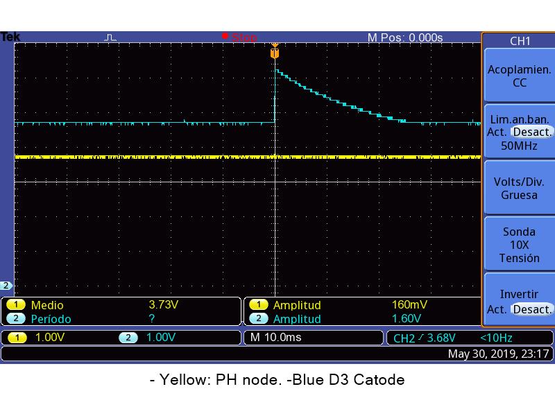
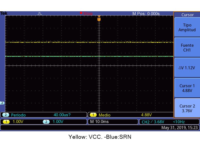
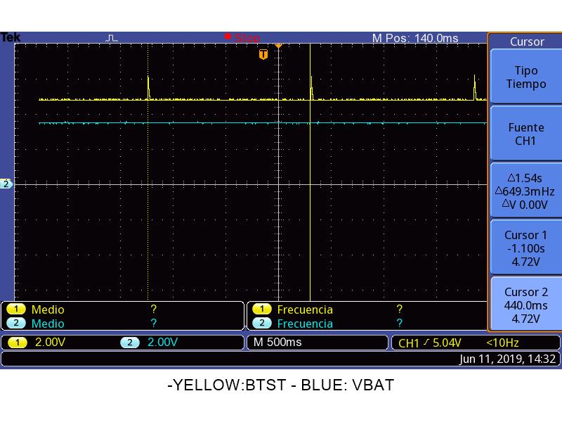
I have taken captures and made measurements of all parameters and the only difference I have found is here.


The measurement point of the picture in my schematic:

The design is based on BQ24650RVM-639 and we did some changes in VMPPSET=4V and also VBat=4.2V.

Any clue what could happen?

Regards

  • Hello,he

    Do you have full schematic of our board?

    Can you also describe your full testing conditions? Are you testing your board with a solar panel or a real power supply? Do you have any loads applied in this test? What is the battery voltage and the regulation voltage setpoint, charge current setpoint, and input voltage capability? What is the input voltage when you measure? What is the VCC voltage as compared to the SRN voltage, as measured from the pins of the charger?

    And what is the waveform you captured? Is that capturing the node w.r.t. ground?

    It would be beneficial to capture on a scope the PH node, the input voltage VCC, the SRN voltage, and the input or output current measurement.


    Regards,
    Joel H
  • I did my tests with 2 differents pcb with the same bench power supply(VCC 5V, 3A) and the same Li-ion battery pack (VBat=3.64V)

    PCB1: Assembled by us in our lab. I've been taking measures before the charge process begin (PCB1_OFFCHG) and when the charger are working (PCB1_ONCHG)

    PCB2: Assembled in China. The same SCHEMATIC, GERBER and BOM.  The main difference is you need to apply VCC= 5.32V in order to the charge process begin.

    Bq24650_Sch.pdf

    The next table shows all measures I took.

    PCB1_OFFCHG PCB1_ONCHG PCB2_OFFCHG
    Vcc 4.8V 4.423V 4.8V
    Vmppset 1.371V 1.371 1.465
    REGN 4.8V 4.39V 4.77V
    Vref 3.29V 3.29V 3.29V
    TS 1.906V 1.906V 1.86V
    Term_En 3.29V 3.29V 3.29V
    Vbat 3.64V 3.84V 3.64V
    VbatReg 4.2V 4.2V 4.2V
    SRN 3.64V 3.88V 3.64V
    Vfb 1.814V 1.93V 1.812V

    Secondly, I've taken some caps of PCB2 in my oscilloscope.

    As you can see in my first post, BTST send "ramps" periodically, however PH node doesn't change.

    In the picture below you can see VCC & SRN:.

    If you need more info and the complete schematic, layout I can upload it without any problem.

    Regards

  • Anybody has an idea about what is happening?

    If someone needs more info I can provide you without any problem
  • Hello,

    It is difficult to say what is different between your two boards. If your prototype is the same as the failing board manufactured elsewhere, I am inclined to note this as a manufacturing error.

    One test we can do on your non-functioning board is to drop the battery voltage during this test to see if this is the result of entering SLEEP mode. Keep your input voltage settings the same (5V), but lower the battery voltage to something like 3.0 to 3.2V and see what happens. 

    Regards,

    Joel H

  • Hello,

    In the table below you can see the values of the next test.

    VCC 4.78V
    Vmppset 1.446V
    Regn 4.78V
    Vref 3.29V
    TS 1.86V
    Term_EN 3.29V
    Vbat 3.43V
    Vbat_Reg 4.2V
    SRN 3.42V
    vFB 1.702V

    In the next picture you can see the "ramps" in BTST node 

    With Vbat=3.43V the device begin to charge at Vcc=5.26V in my power supply and the btst send ramps each 1.5s aprox.

    Should I supose the device is in SLEEPING MODE?

  • Hello,

        From the test results, BQ24650 is not in sleep mode as the condition for SLEEP is VCC-SRN < 500mV. Make sure to measure VCC and SRN on the respective pins of the IC. Your REGN voltage is a lot lower than is specified for this IC and should be between 5.7V and 6.3V with a typical value of 6V. REGN is used to drive the HSFET and LSFET. Can you check for the value of REGN on the boards of yours that were working? If REGN is so low it means IC could have been damaged. Try replacing the IC on failing boards, as well once you have measured REGN on passing boards.

  • Hello,

       We have not heard from you in a while, and assume you were able to resolve your issue. If not feel free to re-open the thread or post a new question.