This thread has been locked.

If you have a related question, please click the "Ask a related question" button in the top right corner. The newly created question will be automatically linked to this question.

TPS54620: the output of the POWERGD status pin is constantly changing, resulting in abnormal monitoring of the status of the pin.

Part Number: TPS54620

Hi,

The enterprise network power project has the following problems when using the TPS54620 power chip:
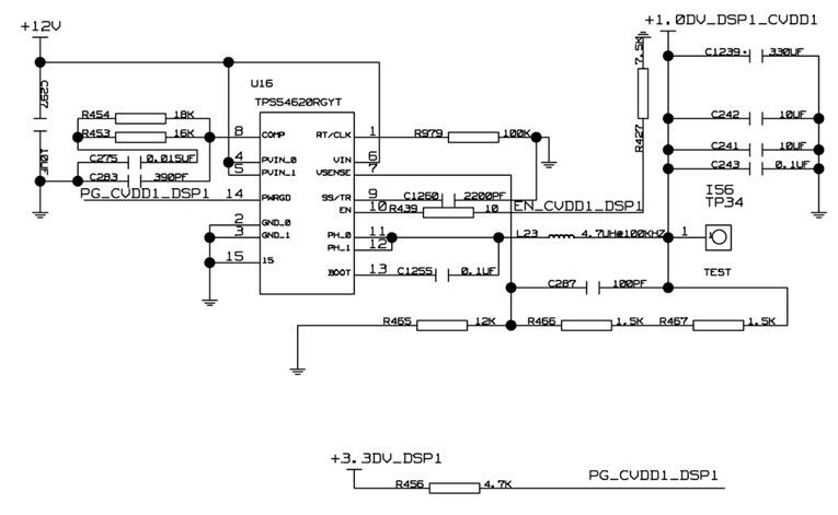
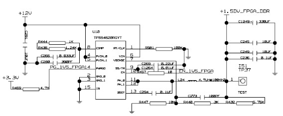
      Two boards appear, using TPS54620 chip, 12V input, 1.0V output, start working normally, after working for a period of time, re-power-on reset, the board works abnormally.
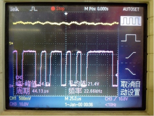
      After testing the board, the 1.0V output of the TPS54620 is normal, but the output of the POWERGD status pin is constantly changing, resulting in abnormal monitoring of the status of the pin.

Why does the chip status pin have a constant transition? How to solve this problem?

  • Hi Elsa,

    I do not see any obvious issues after reviewing the schematic. The only potential one is the inductance is relatively large. This may or may not lead to some stability problems. It may also hurt the response when the load turns off.

    Can you provide a few waveforms using an oscilloscope when the issue occurring? There are two specifically I would like to look at.

    1. VOUT and PWRGD. Please measure the VOUT voltage AC coupled across the output caps with around 50 mV/div. I want to verify there aren't any spikes that may be causing the VSENSE voltage to reach the PWRGD fault thresholds.
    2. PH pin voltage. Please measure with a timescale of around 2 µs. I want to see if the PH pulse-width is stable or not.

    Thanks,
    Anthony

  • Hi Anthony,
    Can't test now. The board has returned to the user by changing the heartbeat.
    The signal was tested in the early stage, and the POWERGOOD signal was always low and the pulse signal was very obvious. The output 1.0V current is large and is available to the DSP TCI6614. And 1.0V is very stable.
    Moreover, the chip also uses this chip to output 2.5V, which works normally. The board is also a problem that occurs after the user has been working for a period of time. Two pieces of state problems have been found.
  • Hi Elsa,

    Unfortunately I don't think there is much I can add to this at this time without any waveforms. As I said in my previous post the schematic is most likely ok but I would like to look at the waveforms I requested to make sure the inductance is not causing any problems with regulating the output. If you see this issue again, please help measure these waveforms with an oscilloscope.

    Also in general the PWRGD pin should only pull low in the conditions described in the 7.3.12 Power Good (PWRGD) section in the datasheet. Have you verified there are not any issues with the voltage pulling up the PWRGD pin?

    Lastly I'm not sure what you mean by the issue was fixed by "changing the heartbeat". Can you explain?

    Thanks,
    Anthony

  • Hi Anthony,

    Has returned to the user, can not test, the status of 2 abnormal boards is not used, the board is normal.
    In the future, the corresponding status pin PowerGood is no longer judged. After the test line test, the board is normal.
    Please evaluate if this solution is appropriate?

  • Without knowing the cause of the issue, I can't say if this is a good solution or not. I recommend finding the cause before deciding on if this is a good solution.

  • Hi Elsa,

    I am going to make this question as resolved for now. If you get more information to help us find the cause of the problem, feel free to reply again to this post and the post will automatically be re-opened.

    Best Regards,
    Anthony

  • Hi Anthony,

    1. The TPS54620 chip uses a total of 10 chips on this board, which generate 1.0V, 1.2V, 3.3V, 1.5V, 2V, 5V, etc., the voltage is normal, other power detection pins PWD are also normal, only 1.0V The POWERGOOG pin is abnormal.
      2. The board that had the problem in the previous period returned from the user. The required waveform was tested with 1.0V output voltage and PWD pin waveform.

  • Hi Elsa,

    It looks like the output voltage has a significant ripple on it and it is likely exceeding the thresholds for PWRGD to go low. The transient response of the 1.0V likely needs to be improved to avoid PWRGD from toggling. A couple things I suggest trying to improve the transient response are:

    1. Decrease the inductance from 4.7 µH to 1.8 µH or lower. This will allow the inductor current to ramp up and down more quickly when the load changes.
    2. Decrease C275 to 4700 pF to improve the settling time of he transient response.
    3. For futher optimization of the compensation, can you share the ESR of the 330 µF?

    Hope this helps.

    Anthony

  • RoHS Compliance.pdfTPE(D2E,D3L,D4 size) .pdfHi Anthony,

    Thanks for your advice.

    And the attachment is the ESR of the 330uF.POS_E 19.pdf

    But why is 1.5v similar design, but no problem?

  • Hi Anthony,

    The Previous picture is 1V, and the 1.5V picture is below:

  • Hi Anthony,

    The Previous picture is 1V, and the 1.5V picture is below:

  • Hi Elsa,

    There are few things I can think of that could contribute to the 1.5V output behaving more normally.

    1. With higher Vout a larger change in the output voltage is needed to exceed the +/- 9% PWRGD thresholds. For 1.0V output it is +/- 90mV and for 1.5V output is it +/-135 mV.
    2. The 1.5V output has much lower gain in the loop compensation (resistor on the COMP pin) so the loop bandwidth is lower. There may be a stability related issue with the 1.0V output.
    3. With higher Vout the inductance is typically larger because the higher Vout ramps down the inductor current more quickly. For example I would suggest 2.2 µH to 3.3 µH as a more optimized inductance for this design.
    4. Does the 1.0V output have larger output load current steps than the 1.5V?

    The ESR is a larger than I had assumed so I will need to update my compensation recommendations for the 1.0V. I also recommend increasing the 390 pF C283 to 1000 pF to better cancel out the ESR zero of the 330 µF cap.

    Anthony

  • Hi Anthony,

    Validation changes were made to the 390 pF capacitor according to the recommendations provided:
    1. Remove this capacitor and the status is normal.
    2. Change this capacitor to 1000pF and the POWERGOOD pin output is normal.
    3. Replace the 390 pF capacitor that was originally removed, and the POWERGOOD pin is also output normally.
    Can you help explain in three cases?

    Thanks

    Elsa Duan

  • Hi Elsa,

    I am a little surprised by a couple of these results. Specifically the first and third.

    First I do not expect the behavior is normal with the 390 pF capacitor removed. I expect the loop bandwidth to be very high and to be unstable without this cap because of the ESR zero from the 330 µF cap. Perhaps the loop was unstable but the high loop bandwidth prevented the output from exceeding the PWRGD thresholds. An easy way to check if the loop is stable or not is to look at the PH node on-time jitter.

    Second It is also strange that behavior was initially not normal with the 390 pF but it was when the 390 pF cap was placed back on the board. Maybe something else was accidentally changed on the board when the modifications were made? Was the exact same test performed for each configuration?

    Anthony

  • Hi Elsa,

    I wanted to check if you needed any further help with this. Just let me know.

    Anthony