This thread has been locked.

If you have a related question, please click the "Ask a related question" button in the top right corner. The newly created question will be automatically linked to this question.

UCC27714: Half Bridge drivers with external FETs to establish our H-Bridge design

Part Number: UCC27714
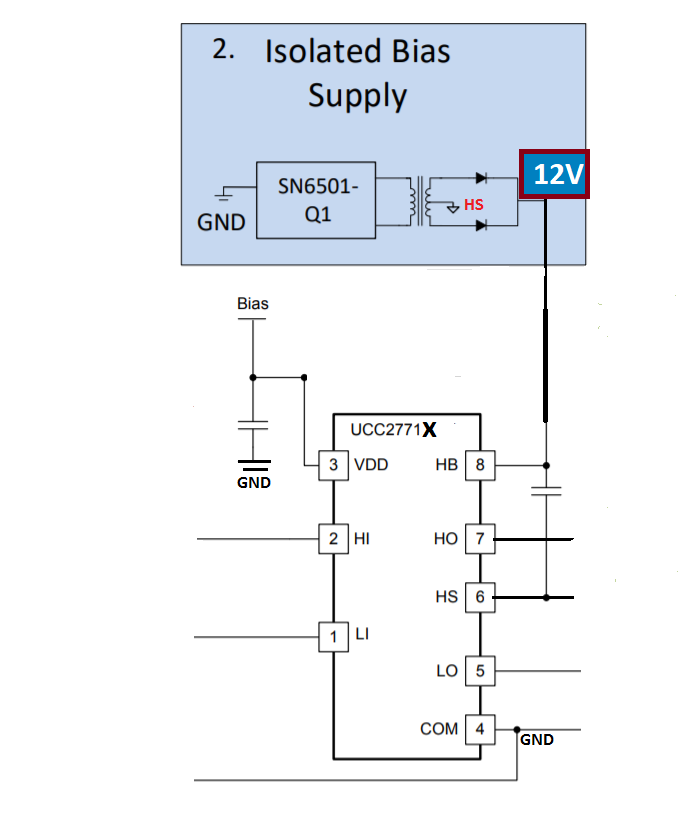
Other Parts Discussed in Thread: SN6501

Hello team,

See below follow-up from customer:

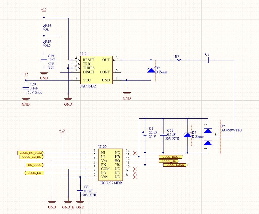
Since we want an adjustable and reversible DC over the load we will use a LC filter between the H-bridge and the load. The filter design is not yet decided but it will be similar to the below versions. Note that there will be internal freewheel diodes in all FET’s that I will use.


  • Will the UCC27714 drivers function as intended with a filter similar to above?
  • I’m most concerned if the boot strap charge pump will still work.
  • Since we will operate with PWM, what do You recommend most, to have the low side FET constant on and we let the high side FET do the switching or do You recommend the opposite?
  • I want to run the driver and charge pump as efficient as possible.
  • It is recommended to have short PCB traces between the driver and the FET’s. What do You consider to be short traces?
  • As of now I may end up with ~5cm long traces.
  • Hi Randhir,

    Thanks for your interest in our drivers, my name is Mamadou Diallo, I am an AE supporting the High Power Drivers group.

    The driver should function according to specs while considering few things:

    -The bootstrap supply needs to maintain sufficient bias to the high side gate to prevent UVLO conditions. If you're considering the bootstrap method, the switch node HS must be pulled to near ground to charge the HB capacitor from VDD in order to replenish the boot cap.

    -Maintaining the high-side constant (while switching the low-side) will require a dedicated bias supply to ensure the HB-HS stays above the UVLO threshold. You can accomplish this by using SN6501 + a small isolated transformer as shown below. This option essentially rules out the bootstrap method.

    -Maintaining the low-side constant (while switching the low-side) will also rule to bootstrap option as HS pin will never find a path to ground in order to recharge the boot cap.

    -I would there recommend switching the low-side FET as this only requires the VDD supply while using a dedicated supply to maintain a constant high-side bias at the FET's gate as shown below:

    I have also attached the SN6501 datasheet below for your consideration.

    -As far as layout, the PCB trace length is proportional to the amount of parasitic in the gate drive portion and inversely proportional to the PCB trace width. In other words, 5cm might be OK but if you can find a way to reduce this length while using wide thick traces (0.7mm to 1mm width) from the driver's output stage to the gate, it will help improve the efficiency and performance of your system. I have attached an app note showing an example of driver and FET placement.

    http://www.ti.com/lit/an/slua964/slua964.pdf

    Please let us know if you further questions or let us know that we addressed your question by clicking the green button.

    Regards,

    -Mamadou

  • Thanks Mamadou. I have sent this over to the customer and will update you once they verify.
  • Hi Mamadou,

    We would have some difficulties to fit a transformer on the board.

    Would attached circuit work?

     I have some difficulties to predict the behavior of C? due to the filter that we will have between the H-bridge and the load.

    Thank You.

  • Hi Stefan, 

    Thanks for following up on this opportunity. 

    I have couple of comments: 

    -For the bootstrap capacitor, please consider using X7R multilayer ceramic capacitor for their stability over temperature and supply range. We do not recommend using electrolytic capacitors as they have significant capacitance shift over temp and voltage range and reduce their effectiveness in filtering noise. 

    Your current bias looks like it is not generating the necessary bias on the HB-HS pin. How did you pick R14, R19 and what is your expected OUT voltage. Have you simulated the circuit?

    As shown below, my simulation shows the OUT pin seems to be stuck on 18mV, I am going to modify it and get back to you as soon as possible.

    Timer.zip

    Thanks.

    Regards,

    -Mamadou

  • Hi,

    I have tried to simulate the circuit but I have had issues with the tools so I have not ben successful.

    I have downloaded the TINA tools and that looks nice. I will give it a try and see how it works for me.

    I opened You file and I think that You get 18mV on the output since the "cont" pin is grounded. It should be floating.

    I have only made this charge pump since I don't think that the charging of the bootstrap capacitor will work when we use the LC-filter described earlier in this thread. We use the filter in order to get a smoothed voltage to our load and my concern is that I suspect that the filter must be emptied every time the bootstrap C is charged and then we kind of loose the purpose of the filter. Do You think my suspicion is correct or do You think that the bootstrap circuit will work as intended even with the LC-filter?

  • Hello,

    I also noticed that I made a mistake in the 555 connections. The trig and threshold should not be grounded but connected above the capacitor.

    BR

    /Stefan

  • Hi Stefan, 

    My apologies for the delay. 

    I have updated the file with Cont pin connected to ground through a capacitor since I cannot directly ground it. 

    Also as you pointed, updated the Threshold and Trigger pins to be connected to charging capacitor C1. By tweaking R1 and R2, you can get the desired charging and discharging times of the high-side FET using the ton=0.693(R1+R2)*C1 and Toff = 0.693(R2)*C1.

    Then you can run the low-side continuously as you had originally planned. Your provision for clamp diodes are also a good idea against transient surges.

    Please let us know if you have further questions.

    Thanks.

    -Mamadou

    Timer_Updated.zip