This thread has been locked.

If you have a related question, please click the "Ask a related question" button in the top right corner. The newly created question will be automatically linked to this question.

TPS7B70-Q1: The output pulse of TPS7B7033 at the case of power down

Part Number: TPS7B70-Q1

Hi,

When we tested  the case of power down for TPS7B7033, there happened an issue about Vout ”MEM_3V3” as followed.

  • Background

    TPS7B7033 is a LDO for the MCU as a constant power. As the schematic is shown in the below picture, DCDC  is sourced from battery(14V), VIN is the input supply for TPS7B7033 which is isolated with DCDC by a diode, while MEM_3V3 is 3.3V level output power from TPS7B7033, which powers for the MCU constantly. EN of TPS7B7033 is the same net of VIN.


  • Issue

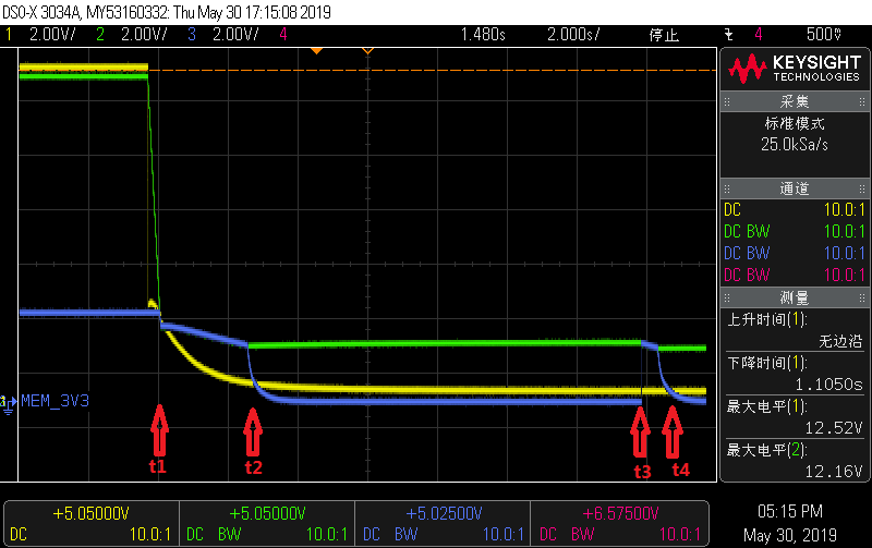
    When powering down the DCDC, we found that the MEM_3V3 went to 0V slowly, then would go up to about 2V strangely after several seconds, a lasting about 440ms pulse is shown in the below waveform.

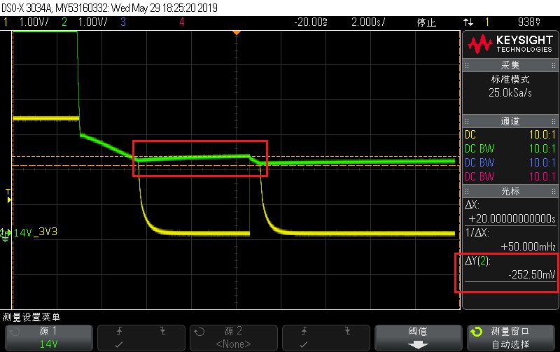
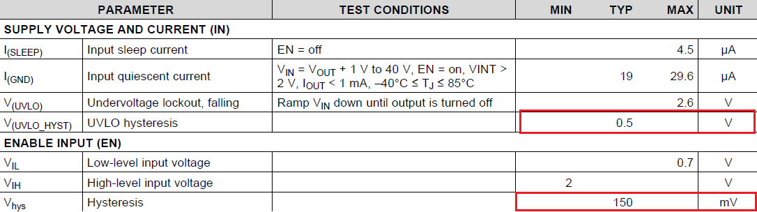
    Power down happened at t1, VIN is followed by MEM_3V3 between t1 to t2, then MEM_3V3 is shut down because the EN pin is disabled at t2. From t2 to t3, why does VIN rise slightly about 150mV at t3 which triggers the EN of TPS7B7033, and then MEM_3V3 follows the VIN again as a pulse? At t3, DCDC goes to almost 0V, so VIN is isolated and can’t be charged by DCDC, My question is: Where and why leads to the VIN rising?

    (Note: Probe1 is DCDC marked yellow, Probe2 is VIN marked green, Probe3 is MEM_3V3 marked blue)

    Do you have any comment on it? Thank you and wait for your reply!


  • Hi Kevin,

    As I have noticed, there is a 1mF capacitor (C1924) at the input of the LDO and this will hold your input voltage for quite some time after DC/DC has been removed. How much load did you have on the output (MEM_3V3)? It seems to me, from the time that DC/DC being removed to t1, the input voltage was dropping dueo to the load at the output.

    Once the voltage at Vin dropped below the UVLO of the LDO which  is around 2.6V, the device was turning the output off. This is why you see at t2, MEM_3.3V dropped to zero. Since LDO is off and the previous load current cannot discharge the output, the input voltage of LDO can only be discharged by leakage, so the voltage stays at/near UVLO levels.

    It seems that when the discharging process is very slow, the input voltage initially hits the somwhere near the UVLO of the device and it trigger the device to shut the output off. Once the output is off, the output was only being discharged by leakage. As this process is very slow for your case with the big input cap, the input voltage enters a grey area that preventing the UVLO circuit to make the consistent decision. UVLO circuit is normally controlled by comparator, and for comparator, there is a grey area that preventing the comparator to make consistent 1 or 0 decisions and this happens to be the case you have in the scopeshot.

    Once output jumps again, the input voltage was discharging a little bit more and the UVLO circuit kicked in again and made the consistent decision to turn off the device.

    Does it make sense?

    Regards,
    Jason Song

  • Hi Jason,

    Appreciate your reply!

    As you described, the output was turned off by the Vin which dropped below UVLO about 2.6V. But I consider that the output was turned off by the Enable pin which dropped to the High-level input value of Enable(Minimum value is 2V), and from the waveform, the value of Enable pin rises about 250mV.Then Vout jumps again because Enable is hit again(Vhys is 150mV).  So this strange phenomenon is caused by Enable pin.

    In my design, Input is the same net as Enable pin.

    So my question is, why the voltage of big input capacitor C1924(1000uF) happens to rise about 250mV to trigger the Enable pin, then trigger the output.

    What's more, I have done another test. I changed value of C1924 to 47uF, the strange phenomenon disappears.

    Expect for your reply!

    Thanks again!

    Kevin Shen

  • Hi Kevin,

    The application has "Enable" and "Vin" shorted together. As "Vin" dropped below 2.6V, the device was still being enabled. The enable threshold  high is 2V, which means when "enable" pin is higher than 2V, the LDO is enabled. In order for "enable" pin to disable the device, the voltage at enable needs to drop below 0.7V which did not happen in your case.

    To answer your questoins,

    So my question is, why the voltage of big input capacitor C1924(1000uF) happens to rise about 250mV to trigger the Enable pin, then trigger the output.

    -- From the scopeshot, I did not see the 250mV rise. Can you point me where the rise is?

    Regards,
    Jason Song

  • Hi Jason,

    See the red marking in the following waveform.This 250mV rising gap confused me a lot. I wonder whether the Enable pin or the capacitor caused this rising gap.

    Thanks a lot!


  • Hi Jason,

    As you mentioned Enable threshold  high is 2V, I think this value is not the real threshold. The datasheet describes the minimum value of Enable threshold is 2V, which doesn't mean the real value is 2V, maybe 2.5V, or 2.6V, or 3V. They are all possible. Why I thinks the Enable pin caused this, the hysteresis is 150mV which causes re-trigger the output While the UVLO hysteresis of VIN reaches 0.5V.

  • Hi Kevin,

    Let me answer your enable threshold question first. The datasheet for EN pin was done in a way  when the voltage at enable pin is less than 0.7V,  the internal circuitry is treating enable as a LOW signal; when the voltage of the enable pin is higher than 2V, it is a HIGH signal. Enable pin voltage here is considerred to be a digital signal and this is, however, the most common way to specify the behaviors of a digital pin. 

    We've had lots of dicussions on how the digital pin like an enable pin should be specified with min and max. I agree it's really confusing sometimes. Sometimes, some digital guys would specify in this way:

    Low level: Min: 0  and high 0.7V.

    High level: Min 2V and high (highest voltage allowed on this pin).

    Do you think this is better than the way it currently is?

    Next time, when we have a discussoin on this topic, I will sure bring your feedback to our discussions.

    Regards,
    Jason Song

  • Hi Kevin,

    This is to answer your questions on the gap. The green is for Vin, as you can see, it's not really rising. I would describe the area you marked in red as a "early UVLO". Considering this as the threshold of  a comparator, when the voltage is dropping, it enters the grey period that comparator is not consistent with its output logic. During the gap voltage area, the LDO's internal UVLO circuit may not have consistent signal that whether the UVLO should disable or eanble the output. Once the circuit has been reenabled, your load will quickly discharge the output voltage to help the voltage pass the grey area and then the UVLO logic turns off the output. Some LDO with UVLO circuit may experience similar behaviors and this one is not alone. 

    Does it make sense?

    Regards,
    Jason Song