This thread has been locked.

If you have a related question, please click the "Ask a related question" button in the top right corner. The newly created question will be automatically linked to this question.

TPS61175: Is there a programmable boost converter solution

Part Number: TPS61175
Other Parts Discussed in Thread: TPL0501-100, DAC7760

Hi, guys. TPS61175 supports voltage output up to 38V.

I was wondering whether there is a programmable solution to change the boost converter's output via SPI, I2C, UART, etc.

Is there a boost converter IC that can change the output like this?

Or should I connect a digital potentiometer like TPL0501-100 to the boost converter to control the voltage output?

  • Dear Sir,

    What is your Vin, Vout, Iout? So that I could select a fit part for you!

    For the boost converter, we can change the Vout by injecting a voltage into the FB pin.

  • Hi, Helen. My bad; I should have specified those parameters.

    Vin: micro USB 5V (4.7~5V)

    Vout: I wish to control this using my MSP432 MCU via SPI, I2C, UART.

    The range is 15~30V.

    Iout Max: 0.1A

    - So I was thinking of using the TPS61175 with a digital potentiometer TPL0501-100.

    - Or hoping to use an alternative boost converter solution from TI

    - Just like TPS61175, I wish to use the ENABLE pin toggling feature. I want to use MSP432's GPIO to turn it on/off.

    - The size/price of the boost converter doesn't really matter.

    - I do not care about the boost converter's efficiency, but I hope this dissipates low heat (50 °C or less) as possible.

    - But I do not prefer Ball Grid Array packages.

    Q0. What will be your suggestions?

    Q1.

    Helen chen said:
    For the boost converter, we can change the Vout by injecting a voltage into the FB pin.

    I never heard of this. May I ask more details about this, please?

  • Hi David,

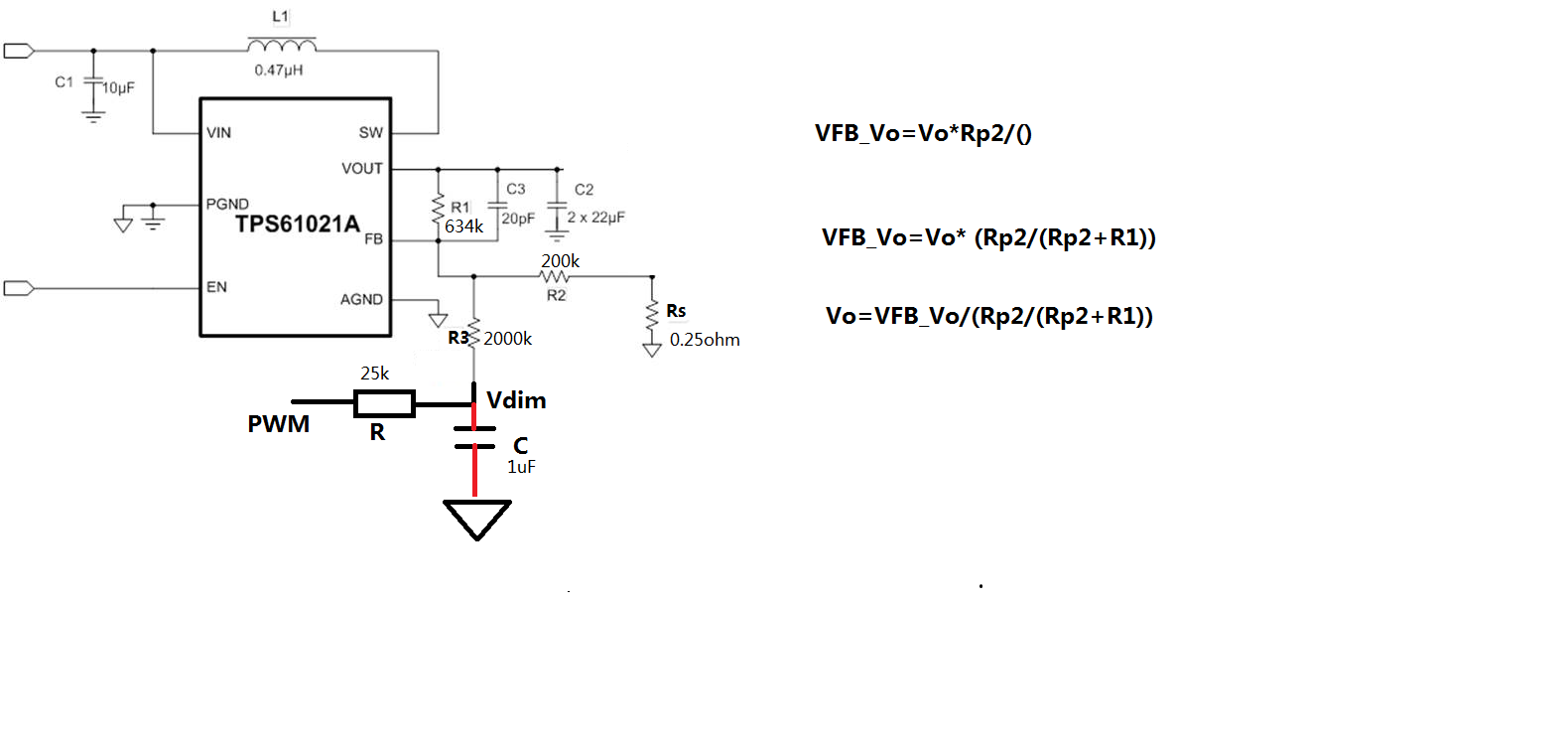
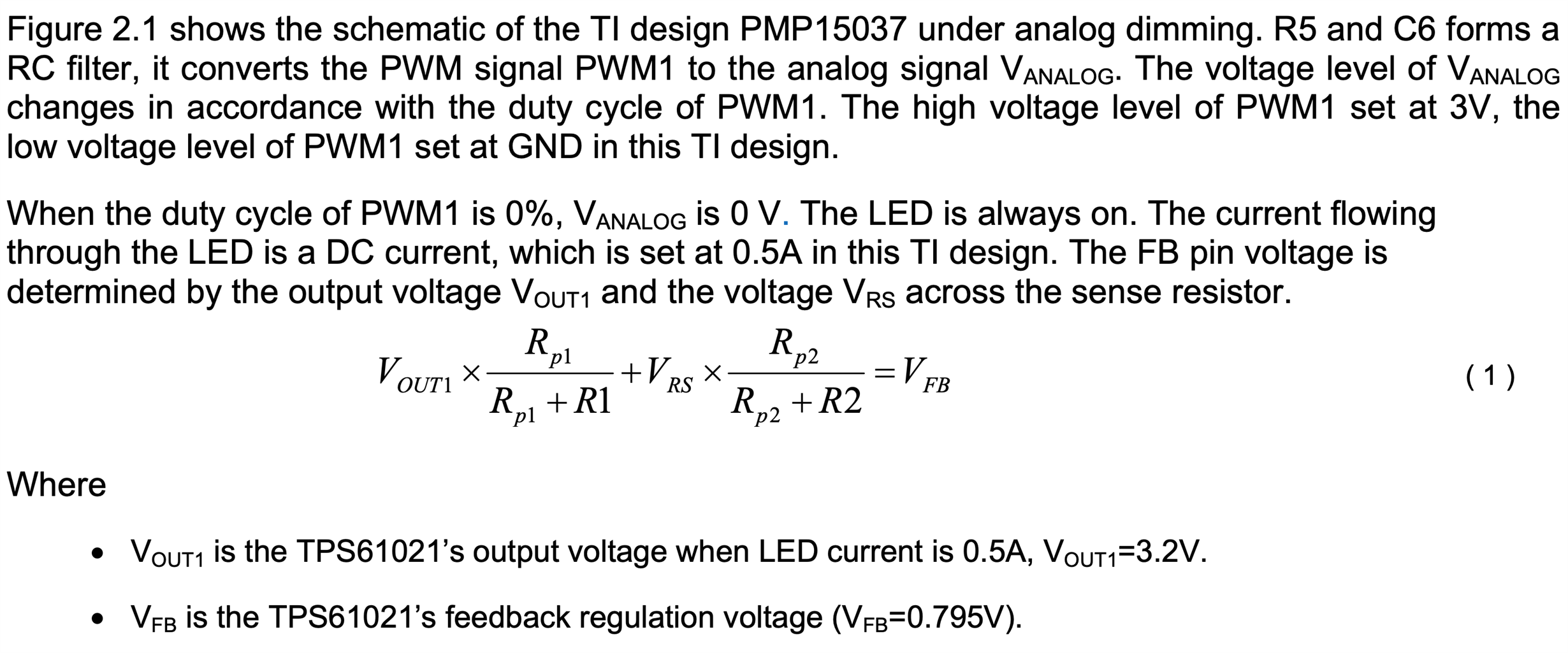
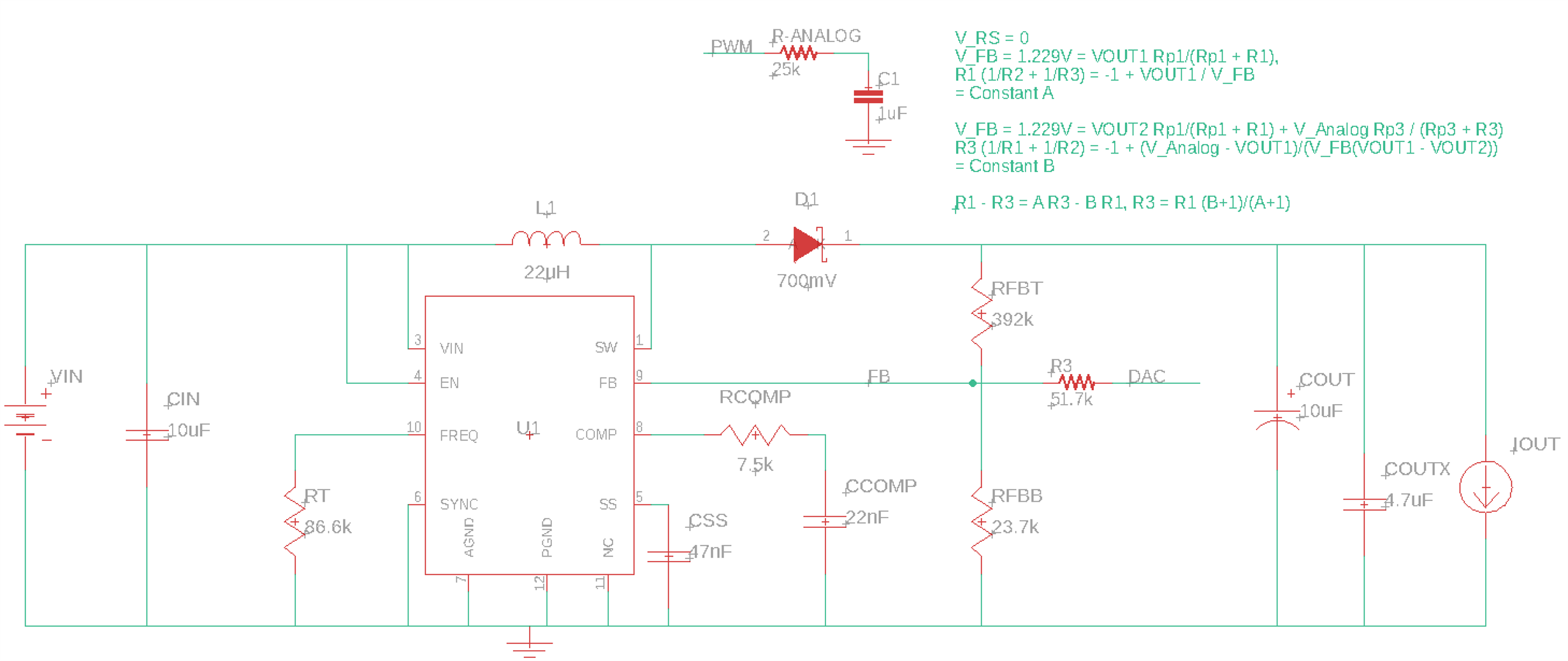
    They can change the output voltage by adding a DC voltage to the FB pin. MCU output a PWM signal, filter it using a RC filter. so you can get a DC voltage changing with the duty of the PWM signal. inject this voltage to the FB pin. You can refer to the below sch for a reference, the concept is the same.

  • Wow, Helen. This is truly interesting!

    Helen chen said:
    You can refer to the below sch for a reference, the concept is the same.

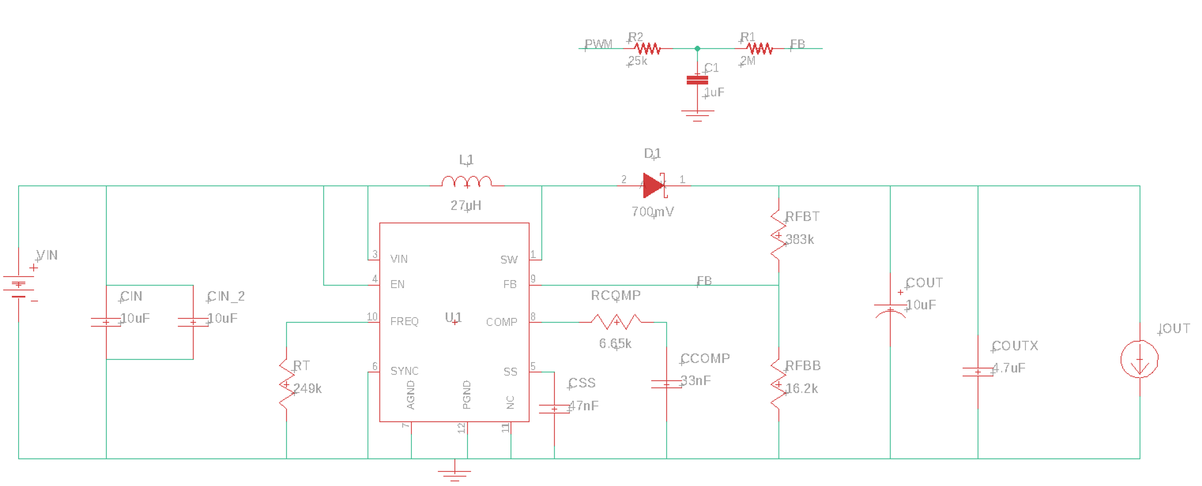
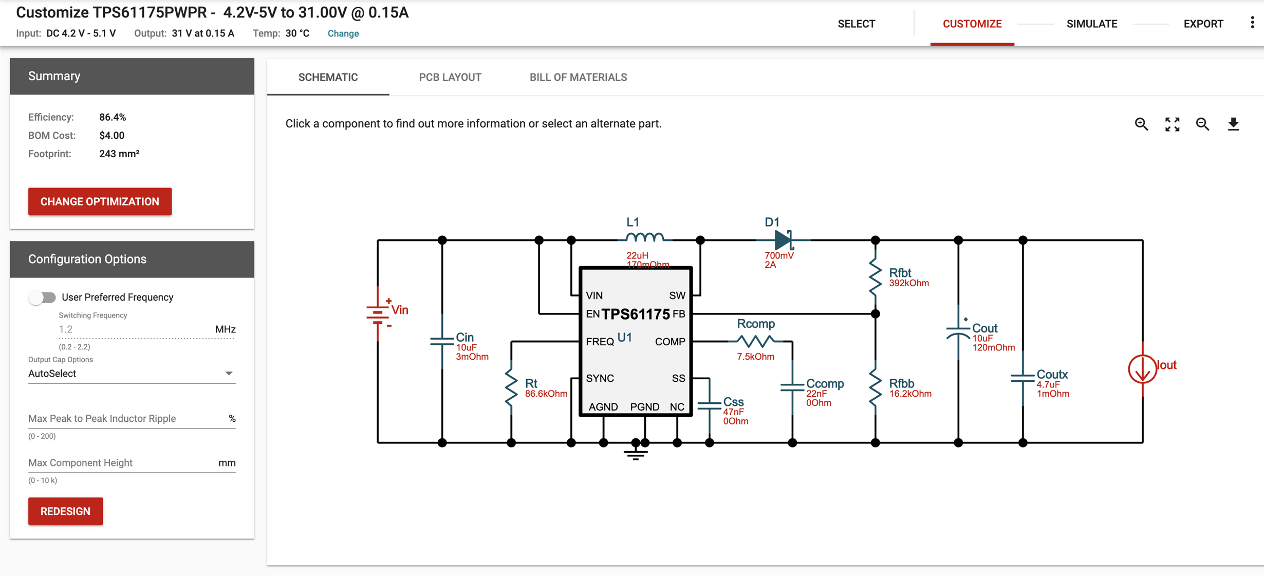
    Q0. Do you mean to create a schematic like this?

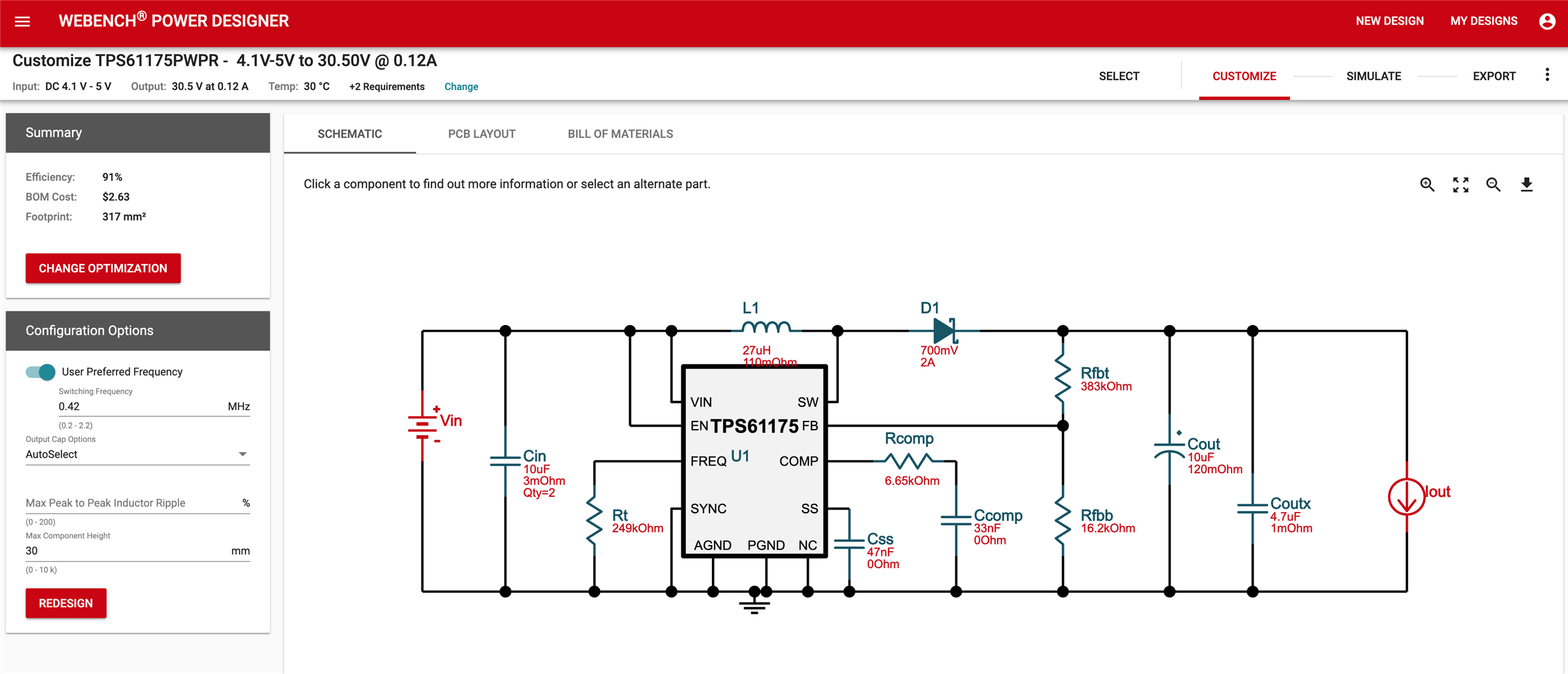
    I referred your design and the WEBENCH design as well.

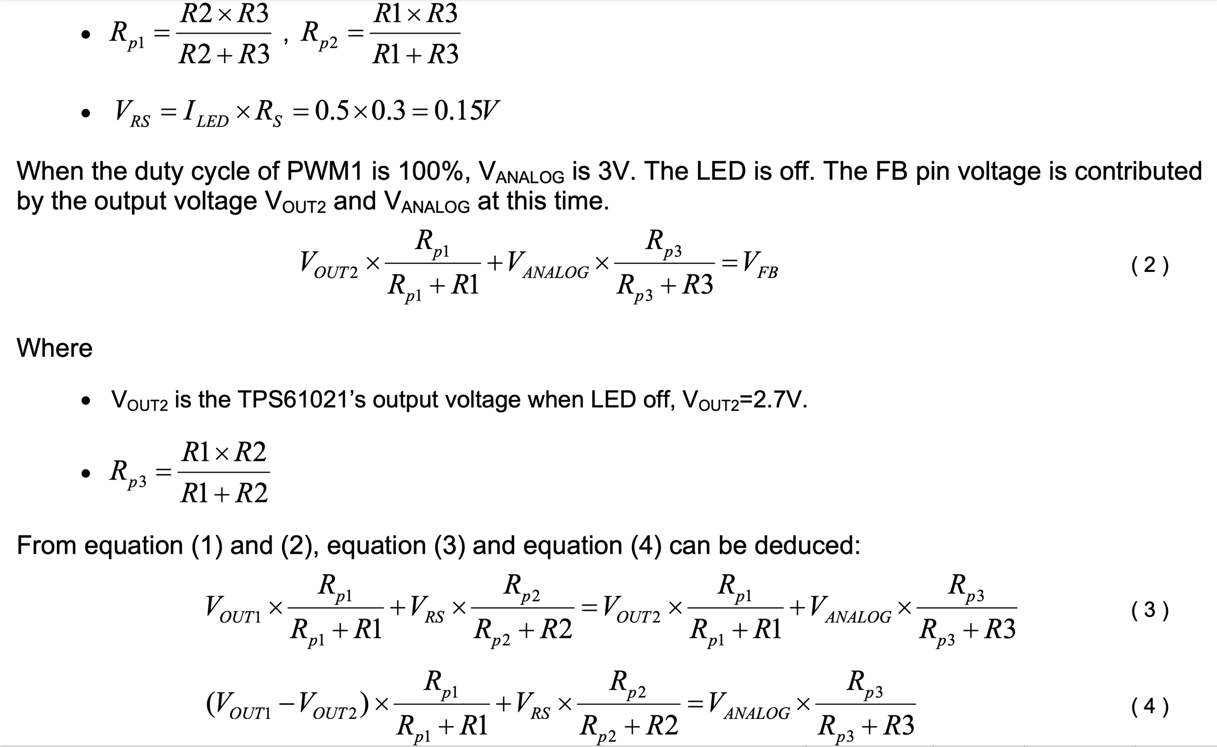
    Q1. In your picture, I don't see Rp2. Can you re-arrange your equation, please?

  • Yes, your circuit is OK!

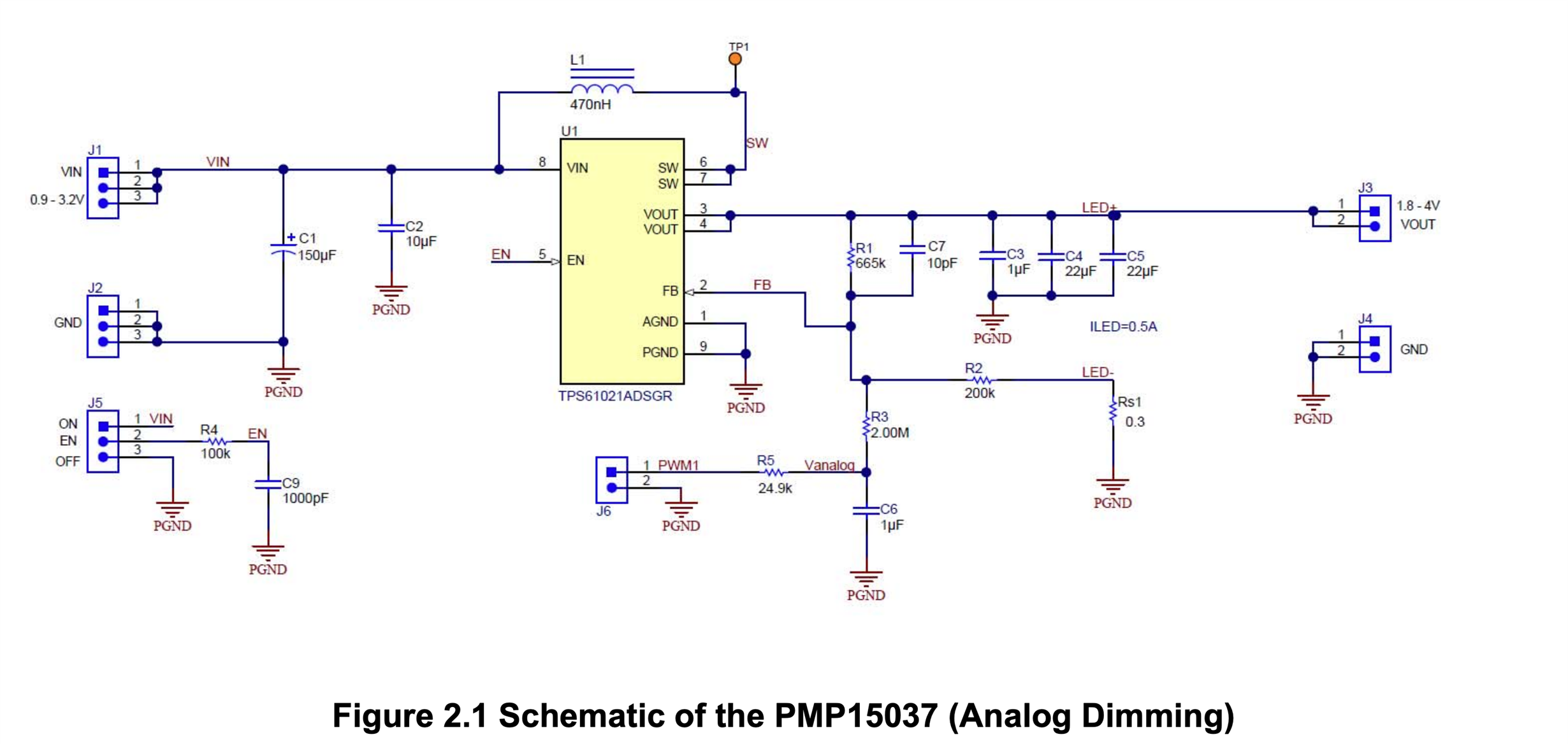
    Please download PMP15037, you can found the definition on page 3.

  • I think this is terrific, Helen! Just a few more things, please.

    I think the concept is to use the superposition of voltages to control V_FB.

    However, in that example, it uses the LED's current to calculate V_RS.

    Whereas for my case, I don't know what value should I set for V_RS and R_RS.

    So my questions are

    Q0. Since my case is a little bit different, how should I set R_RS and V_RS?

    Q1. For my case, should I set VOUT1 = 30.50V for PWM 0% duty cycle and VOUT2 = 3.6V for PWM 100% duty cycle?

    Or the opposite, VOUT1 = 3.6V and VOUT2 = 30.50V?

    Q2. In equation 1, it says "VFB is the TPS61021’s feedback regulation voltage (VFB=0.795V). "

    Does this mean VFB, for both TPS61021 and TPS61175, is constant or fixed?

    If not, I wish to know VFB was calculated.

    After this, I think I will be able to calculate

    R1, R2, R3 using Excel

    https://www.hec.ca/en/cams/help/topics/Solving_equations_with_Excel.pdf

    Thanks for everything.

    P.S.) I haven't received your reply from my other thread.

    I hope you can take a look Helen, please.

  • Dear Sir,

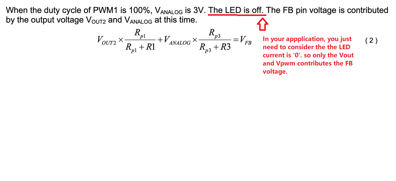
    You just need to consider the LED currents is 0.

  • Dear Helen.

    Helen chen said:
    You just need to consider the LED currents is 0.

    I see. However, I'm still having trouble how to set the values. Because for equation 1, the LED 1 is on so I think there are other considerations.

    Q0. Since my case is a little bit different, how should I set R_RS and V_RS?

    Q1. For my case, should I set VOUT1 = 30.50V for PWM 0% duty cycle and VOUT2 = 3.6V for PWM 100% duty cycle?

    Or the opposite, VOUT1 = 3.6V and VOUT2 = 30.50V?

    Q2. In equation 1, it says "VFB is the TPS61021’s feedback regulation voltage (VFB=0.795V). "

    Does this mean VFB, for both TPS61021 and TPS61175, is constant or fixed?

    If not, I wish to know VFB was calculated.

  • Hi David,

    For the TPS61175, VFB=1.229V.  Different IC has different VFB.  Vout1 and Vout2 is your two target output voltage.

  • Thanks.

    Helen chen said:
    Vout1 and Vout2 is your two target output voltage.

    Q0. My desired range is 3.6 ~ 30.50V. Should I set VOUT1 = 30.50V for PWM 0% duty cycle and VOUT2 = 3.6V for PWM 100% duty cycle?

    Or the opposite, VOUT1 = 3.6V and VOUT2 = 30.50V?

    Q1. How should I set R_RS and V_RS?

  • Hi David,

    What is your Vin? Vin should be <Vout1=3.6V. or you need to use Sepic instead of Boost.

    @ 0% PWM duty, Vout reaches the highest value 30.5V,  while @ 100% duty, Vout reaches the lowest value 3.6V.

  • Helen chen said:
    What is your Vin? Vin should be <Vout1=3.6V. or you need to use Sepic instead of Boost.

    I wish to make a correction for my previous input.

    My desired VOUT range is 6 ~ 30.50V.

    The Vin is 5V by using the micro USB. How should I set R_RS and V_RS for this case?

  • Dear Sir,

    Since you needn't sense the current, so RS=0 ohm, V_RS=0V.

  • Thanks, Helen! I did some math.

    After referring the WEBENCH design, I fixed R1 (RFBT) to 392k Ohm. I also used the equations from the reference design PMP15037.

    By setting VOUT1 (0% PWM, max voltage) = 31V and VOUT2 (100% PWM, min voltage) = 6.5V, I got

    R2 (RFBB) = 23.55964641 k Ohm

    R3 = 51.68 k Ohm

    By choosing

    R2 = 23.7 k Ohm

    R3 = 51.7 k Ohm

    I expect to get VOUT as 6.38477145 ~ 30.87529369 V.

    I have 3 questions left before closing this.

    Q0. Is my calculation and schematic connection correct?

    Q1. I can use the boost converter TPS61175 for this, not the Sepic, right?

    Q2. I have the TI's dac7760 DAC chip on my custom PCB. Instead using PWM and the low pass filter, which was connected to R3 for PMP15037,
    can I connect a DAC output instead to R3, just like my schematic?

  • Dear Sir,

    Your calculation is OK. You can get 30.8V output if the PWM=0% and 6.4V output when PWM=100% and the PWM high level =3.2-3.3V.

    If the DAC is a clean DC voltage, then it is OK to connect to R3.