This thread has been locked.

If you have a related question, please click the "Ask a related question" button in the top right corner. The newly created question will be automatically linked to this question.

TINA/Spice/TPS82130: TPS82130 Inverting Buck-Boost Topology

Part Number: TPS82130
Other Parts Discussed in Thread: TINA-TI,

Tool/software: TINA-TI or Spice Models

hi!

TI,

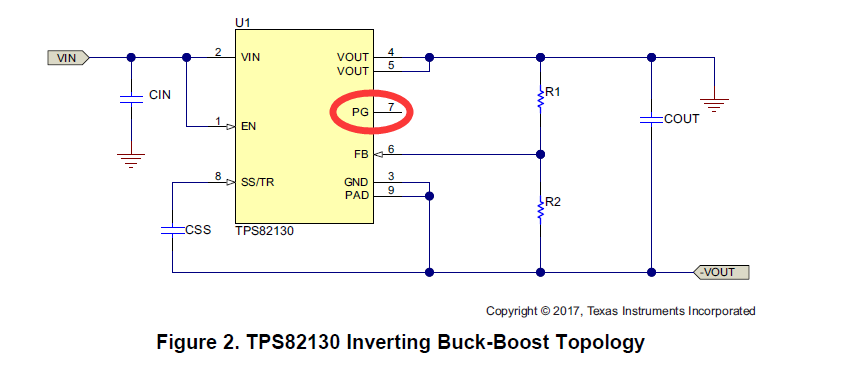
I have a question about TPS82130 Inverting Buck-Boost Topology .

1.in TPS82130 datasheet,CIN connect  to the -vout

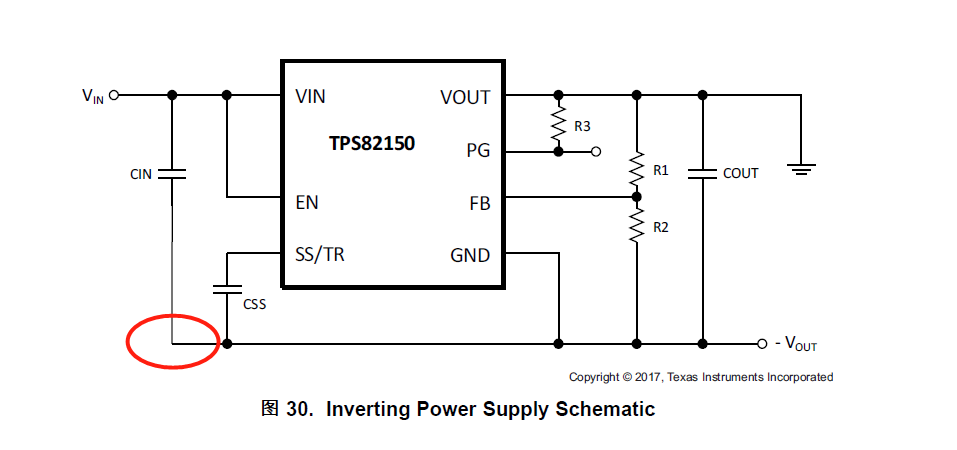
2.in the sheet TIDUCV2, CIN CIN connect  to the  GND
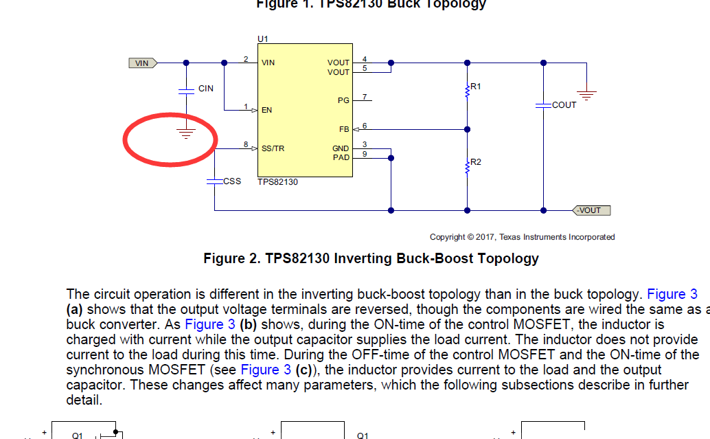
3.My question 

a.Which of the above two situations is right? 

b.What is the essential difference between the above two situations

Look forward to your reply !thanks very much

  • Hello,

    That's a good point! This topic is discussed in the TICUCV2 in the Input Capacitor selection topic (1.4.7).

    We do not recommend the use of a capacitor from Vin to -Vout, because it provides an AC path from Vin to -Vout, a current is created and need to go back to ground to complete its loop. This current could flow in the body diode of the low-side MOSFET and damage the part if no appropriate external component is placed such as a schottky diode.

    Both implementation are correct if extra attention is given to the first one, nevertheless I would recommend you to follow the second schematic.

    If you have any further questions, please ask.

    Thank you for reaching out us!

    Best Regards,

    Dorian


  • HI!

     Dorian

     Thank you very much for your reply. 

    I have another question for you. 

    1.In my design,  TPS82130 output  is -1.8V,I want to monitor the existence of this voltage. I want to connect the pg signal to mcu. But, the TPS82130 Inverting Buck-Boost Topology,The pg signal is not connected. 

    2.My question 

    a : the TPS82130 Inverting Buck-Boost Topology,The pg signal is used as the TPS82130 Buck Topology?

    b:the TPS82130 Inverting Buck-Boost Topology,the Pg signal pull-up resistance to +3.3V ,and connect to mcu,Is this all right? 

  • Hello,

    This PG pin is not only use in the buck-topology. 

    Does your mcu withstand negative voltages at its input ? As VOUT is the IC ground in this configuration, the PG pin is referenced to VOUT instead of ground, which means that the TPS82130 device pulls PG to VOUT (-1.8V) when it is low and 0V when it is high.

    If not you will have to had extra components so your mcu can process the PG signal. 

    This topic is discussed in the  same TICUCV2 in the Power Good Pin Configuration topic (2.3.5).

     Also, the PG pin should not be driven more than 6 V above the negative output voltage to avoid violating its absolute maximum rating. In this configuration with a -1.8V output and a pull-up resistance to +3.3V, your system is good to go if the mcu's input enable negative voltages at its input.

    Thank you very much!

    Best Regards,

    Dorian

  • HI!

     Dorian!

     Thank you very much for your reply,I see.