Dear all,
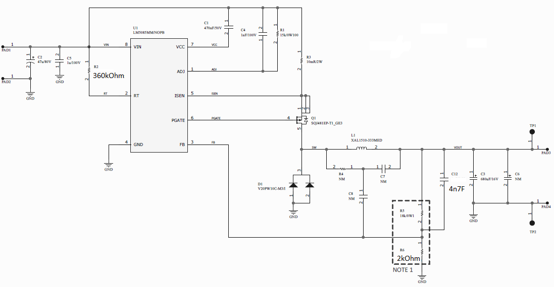
I'm trying to reduce the size of a previous buck converter designed unisg the LM5085. My design parameters are:
24V < Vin < 65V
Iout_nom = 10A
Iout_min = 0.5A
Vout = 12.5V
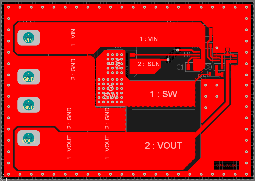
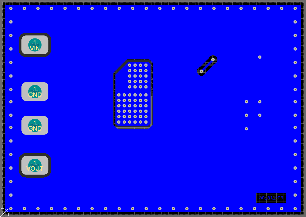
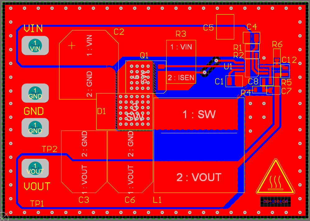
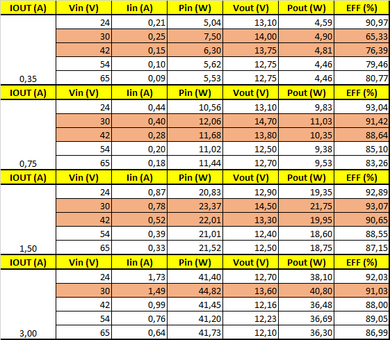
By following the schematic attached, I've drawn the layout also attached. During the validation (I've stooped in IOUT = 3A), I've noticed and erratic behaviour of my converter in Vin = 30V because VOUT raises 2.5V approximately and from here comences to decay to 12V (see attached table). in different VIn, the buck converter works fine!
Do you think I've EMI problems? There's one think I hate the most about my layout, PGATE and ISEN cross each other in different layers. Do you think thi's is a big issue??
Many thanks,
David