This thread has been locked.

If you have a related question, please click the "Ask a related question" button in the top right corner. The newly created question will be automatically linked to this question.

TPS54335A: how to reduce the Vout ripple in a buck circuit

Part Number: TPS54335A
Other Parts Discussed in Thread: LMR14010A

Hello: 

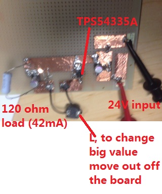
I need help for the buck circuit using TPS54335A (22V~26V input, 5.1V3A output)

I made a prototype based on the export files from WEBENCH Design Center. I use all recommended part-number-parts it suggests.

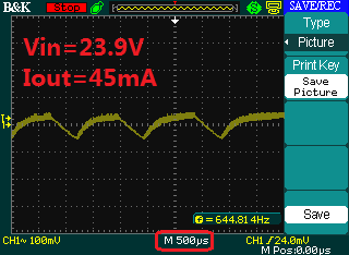
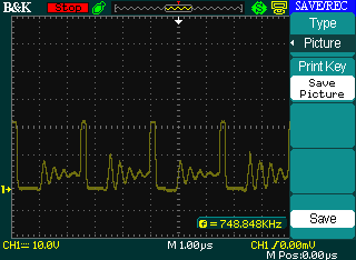
At no load, Vout(max)=5.20V, Vout(min)=5.04V Vpp=160mV,  The waveform is not frequency related.

I add another 270uf Cout, doesn't help.

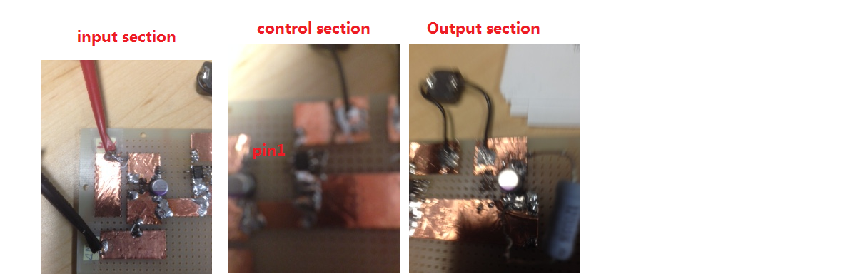
Further look at the prototype, I find the 24V input has 400mV ripple. In this circuit, the Vin and Vout share the same GND. I add a ferrite beads between GND(Vin) and GND(Vout) , doesn't help.

For Vin, 400mV at 24V nominal, 0.4V/24V=1.66% is acceptable.

Any suggestion will be highly appreciated.

Thanks.

Regards;

Chang Cao

  • Hi,

    Could you please share the schematic? If you use electrolytic capacitor, the output ripple would be larger.

    Shawn

  • Hi, Shawn:

    I build prototype following the WEBBENCH design, On last page it says Vout p-p= 7.678mV. All parts used are the same P/Ns in BOM except I change 0201 R package to 0603. see attachment. In the next post, I will send you the waveform of ripple.5.1V3A schematic.pdf

  • I attach the ripple waveform. the 1mm-1.5mm-1mm-1.5mm...... ripple is not switching frequency ripple (Rt=127K, F should be ~500K). Where does this 1mm ripple come from? The HighFrequenyRipple is superimposed on the 1mm period ripple (on the rising edge), is it the switching F ripple, seems match the WEBENCH file Vout p-p= 7.678mV

  • I notice that this time the slow frequency has equal period 1.25ms, before(in 3 days), it is always 1ms--1.5ms--1ms--1.5mm... I take my prototype photo again for you to analysis. I added 2 ferrite beads to isolate Vin and Input GND, doesn't help. I use jump wires to short them. Also I add ceramic cap 10uf + 0.1udf, doesn't help, removed.

  • I am wrong. the ripple frequency has nothing (less) to do with switching frequency. The I(L) can't be suddenly changed, so roughly take it as constant.  the ripple frequency mainly depends on Cout and Load R. (in my case, it is 120 ohm resistor),

    But I did add 3 Cout (total 4 x270uf = 1080uf), the ripple only drop from 160mV too 130mV.

    Here has a problem: Our application is to stepdown 24V DC to 5.1V to power a single-board computer, the load is not constant (don't know it is resistive load or combination). sometime it is heavy and sometimes it is light light. Will this circuit fit our application? if not, would you please recommend a buck circuit for us?

  • Hi,

    The load current is about 45mA, the IC works in Eco-mode, the switch frequency is lower and inconstant, not 500kHz. The IC increases efficiency by reducing the switch frequency at light load. The output ripple would be larger because of the low frequency.  You can try to change 120ohm to 5ohm, the ripple is lower and the switch frequency is 500kHz. 

    There is no problem for your application, it is okay for the light load and heavy load.

    Shawn

  • Hi, Shawn:

    yesterday evening I shunt another 120 ohm resistor to the load, Iout = 5.1V/60 ohm = 85mA, the ripple p-to-p drops to 45mV. I plan to add a 60 ohm 1.5W dummy load to eliminate light load big ripple.

    Now I am trying to test full load ripple and heatrise.

    Another question: We will use the same 24V as Vin of  two bucks: one is 5.1V3A and the other is 12V1A (the circuit will be the WEBENCH design using LMR14010A. Will the 5.1V buck load change affect 12V buck performance? Do I need to add some decoupling network between 24V and two Vins?

    Thanks.

    Chang

  • Shawn:

    Unfortunately  as I put a 3.75 ohm load (5.1V/3.75 ohm = 1.36A) and turn on 24V Vin, it causes short (Vout to GND). the chip pin3 shorted to pin4. What possible reason to cause this short?

    Thanks.

    Chang  

  • Hi, Shawn:

    I change the chip.

    At no-load and 60 ohm load,  it is okay.

    As I put the 3.75 ohm load, short happens as I turn 24V Vin ON. Is the 24VDC power supply related? I use Instek Laboratory DC power supply Model: GPS-3030DD (0~30V, 0~3A). Will it cause big inrush current? but not Vin (pin2) short to GND(pin4), it's PH(pin3) short to pin4. 

    Thanks.

    Chang

  • Hi,

    The layout of your board is bad, the spike voltage of PH is very large which would lead to damage of Low side MOSFET. You can check the waveform of PH.

    Shawn

  • Thanks.

    I will re-build the prototype.

  • Shawn:

    I rebuild the prototype, still no good.

    At 60 ohm load(5.1V/60=85mA), I measure the PH waveform as attachment, which is similar to TPS5433xA Page33 Figure 31 (but the low ripple is big).

    When I add load 3.75 ohm (5.1V/3.75 = 1.36A, half load), the chip is damaged : pin2(Vin) and Pin3(PH) shorts to GND (pin4)

    What next I should try.

    Thanks.

    Chang

  • I replace the chip 3rd time. This time , with 3.75 ohm load, unlike previous cases, it immediately broke. this time the output is only 1.23V, and last for a couple of minute, then break.

  • Hi,

    Please set the bandwidth of oscilloscope to 500MHz when you test the SW waveform, I think the spike voltage would be large.

    You can try to add a 0.1uF ceramic capacitor close to VIN pin and GND pin of IC to reduce the spike voltage.

    Shawn

  • Hi, Shawn:

    I re-built  prototypes, all broke (I broke 7 chips)  at 3.75 ohm load (5.1V/3.75=1.36A half load).  Today I follow the suggested layout in the datasheet page 39, the main difference from my previous layout is PH goes to bottom layer. It does improve. Now 1.36A is okay. however when I use load 1.875 ohm (2.72A), the Vout is 1.2V and in several seconds, it broke again.

    I really feel bad.

    What else I can do?

    Thanks.

    Chang

  • Chang Cao said:

    Hi, Shawn:

    I re-built  prototypes, all broke (I broke 7 chips)  at 3.75 ohm load (5.1V/3.75=1.36A half load).  Today I follow the suggested layout in the datasheet page 39, the main difference from my previous layout is PH goes to bottom layer. It does improve. Now 1.36A is okay. however when I use load 1.875 ohm (2.72A), the Vout is 1.2V and in several seconds, it broke again.

    I really feel bad.

    What else I can do?

    Thanks.

    Chang

    I attach the new layout.

  • I have 0.1uf cap at Vin, but can't as close as to the Vin pin.

  • I only have one chip available. I will try to build another prototype to measure the inrush of SW. After that, I need to wait (I purchase chip and wait for receival)

  • I notice that the compensation network has different  RC values between WEBEBCH design (which I use) and the sample schematic in datasheet.

    WEBENCH design (54335A): Rcomp=23.7K, Comp=560pf, Comp2=51pf

    Datasheet (54336A): Rcomp=3.74K, Ccomp=12nf, Ccomp2=120pf.

    Do 54335 and 54336 have the same die structure? will the compensation network poles/zero affect the buck performance? especially for the heavy load conversion?

  • I measure the PH waveform as below. Before I further increase the load, I decide to measure the Vin pin waveform incase it shorts at heavy laod. Unfortunately, during I probe the Vin pin, I short it and damage the chip again. now no chip can be tested, have to wait for newly order chips coming.

    Thanks.

    54335 chip is so valunable, should I change to another chip?

  • Hi,

    I can't see the attached waveforms, it seems there is something wrong. Could you please upload it again?

    TPS54335 and TPS54336 are almost the same for the internal structures, for the compensation values, they are related to the VIN, VOUT, switch frequency, L, Cout. 

    I think the the root cause is that the layout is bad, the SW spike voltage is too large. You can try to decrease the input voltage to 12V,18V, 20V to check it, and test the SW waveforms.

    If you change the layout, try to place the 0.1uF capacitor close to VIN pin and GND pin. Or you can place the 0.1uF cap on the chip, and close to VIN and GND pins, then solder them together.

    Shawn

  • Shawn:

    my coworker gave me a piece of TPS54335A and build another prototype, It seems the Vin ripple is too big.

    PH waveform is as below:

    Input voltage Vin ripple: Obviously the Vin ripple, especially at chip side increases bigger and bigger, this may be the cause for heave load damaged. I will add another 0.1uf or 0.01uf cap to see if the ripple can be reduced. Once the ripple is reduced, I will increase the output load.

  • I add 0.1uf and 0.01uf caps, doesn't help.

    I check the datasheet, 6.1 Absolute Maximum Rating The Vin ripple seems not relevant.

  • Scope shows VIN, BOOT, VSENSE, COMP, RT , PH amplitude all are in range with some margin. at Iout=1.092A

    So what is the root cause to cause chip shorted at heavy load?

  • Hi,

    I can't see the waveforms.

    As I mentioned, you need to check the SW waveform, to see whether the spike voltage is too large, and the bandwidth of oscilloscope should be 500MHz.

    Shawn