This thread has been locked.

If you have a related question, please click the "Ask a related question" button in the top right corner. The newly created question will be automatically linked to this question.

TPS63070: TPS63070: Max Duty Cycle not specified? Also, WEBench appears to be wrong.

Part Number: TPS63070
Other Parts Discussed in Thread: TPS63802, TPS61089, TPS61022, TPS61088

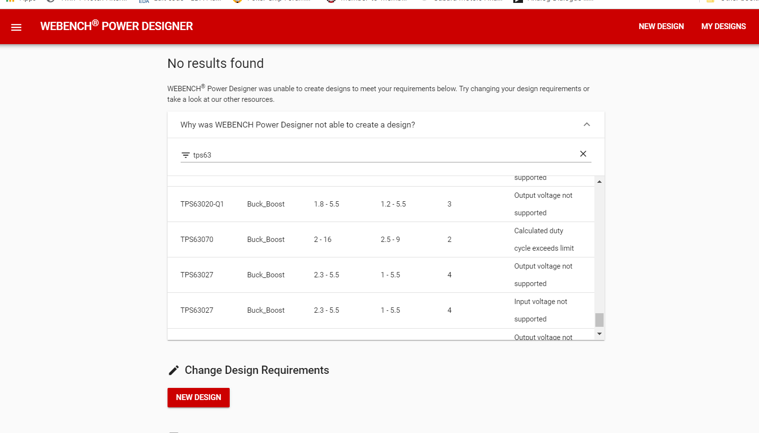
Here are my design parameters using a TPS63070:

Vin   = 2.0V - 3.2V
Vout = 6.2V
Iout  = 1000mA 

Assuming 80% efficiency in boost mode, duty cycle D = 1 - [Vin,min x efficiency]/Vout  = 1 - [2.0x0.8]/6.2  = 74.2%

When I plug in the above numbers into WEBench, the online tool reports back that a design cannot be made due to "max duty cycle".  However, the TPS63070 does not have a max duty cycle specified in the data sheet;  so, this leaves me to wonder (a) Why is no max duty cycle specified in the data sheet?  (b)  Is it really the max duty cycle that is limiting this design?  

Also, when I run the numbers for switch current inside TI Power Stage Designer, I find that the switch current stays below the 3.6A limit:

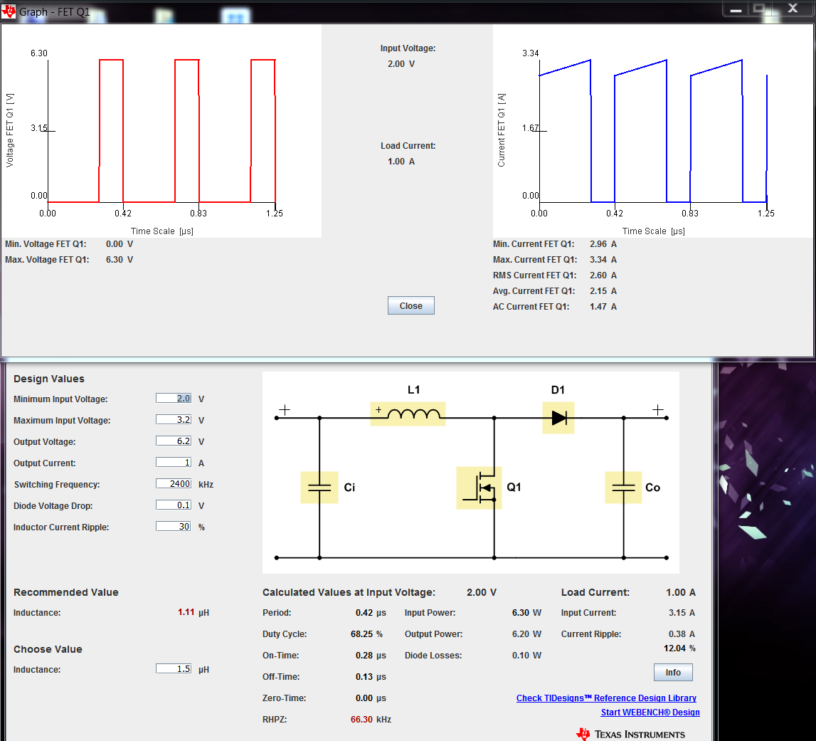
Hand calculations more or less match the above results +/- a few percent. 

I'm confused.  It feels like I am missing something here because one set of tools and hand calculations are saying the design is possible with this PMIC, but WE Bench tells another story.  What is the true reason the TPS63070 cannot handle the above conditions?

  • Hi Adam:

    I thought it's caused by the current limit. Iin=Vout*Io/Vin/Eff=6.2V*1A/2V/80%>4A. It's exceeded the limit list in spec.

    You could have a look at TPS63802 with larger current capability. But it's still hard to support 1A/6.2V @VIn=2V.

    May you tell what's the application it is, and does it need 1A output current for all Vin range?

  • Hi Adam:

    I have checked with the team. The TPS63802 couldn't support the 1A/6.2V.

    May I know will you accept to use a boost converter? It seems more suitable for you spec.

  • It is acceptable to use a pure boost converter in this application, yes.  Preferable, actually.


    Integrated switch & synchronous rectifier are preferable.
    But it would be possible for us to use an external switch, if no integrated switch PMIC exists.  That is always an option.
    We are most concerned with the IC package size.   It seems that many of the "external switch" PMICs are MSOP or SOIC size packages, which are way too large for us.

    Ideally we need a 3x3 DFN solution.  3x4 is doable;   4x4 is probably the max that can be supported in the PCB real estate we have. 


  • Hi Adam:

    Do you mean you need different Vout change function for you application?

    May you share some more details information to us? As what's the Vout range, other functions you need. So that we could recommend proper device for you. Thank you~

  • Another question: 


    Specification on the TPS63070 state VIN "for start up", Vout < 3V  is minimum 3.0V

    Does that mean this converter will not start up with an input voltage < 3V, at all? 

    What about when is Vout > 3V?   Will this converter start up with Vin = 2.0V, 2.1V ? 

    I'm asking this because when I move my input voltage to 2.5V and flip the EN pin high, I am getting intermittent start up or no start up at all.  I don't understand why this is even a design characteristic at all ... 

  • Hi Adam,

    as the input voltage is always lower than VOUT, boost converter should be better solution. However, there is not a boost can work on this application as the input voltage is down to 2V and VOUT is up to 6.2V. we have TPS61022 support this power and low input, but output is less than 5.5V. we have TPS61089 support 6.2V output, but can't support 2V input.

    we have a reference design for similar application, http://www.ti.com/tool/PMP9772 . a low input/power boost for the power VIN of a high input/power boost.

    the low input/power boost could be TPS613222A, and the high input/power could be TPS61089 or TPS61088.

  • Hi Adam:

    I just answer your question about the TPS63070 startup condition. Please also look at Jasper's suggestion.

    Please realize that there is a under voltage lockout function for this device, and the rising hysteresis is 850mV typically. So even the Vout above 3V, the minimal input voltage should be higher than 2+0.85=2.85V typically. 

    The hysteresis will be influenced by many factors. You could check the details range in the datasheet.

  • Hi Adam:

    How is it going? May you share some updating?

    Please let us know if you need further support. Thank you~

  • Hi Adam:

    I closed the thread assuming that you had solved the issue. if not, just reply below