Other Parts Discussed in Thread: BQ24040, SN74AUP1G80
Apologies for my 3rd post concerning TPS22933 ;) I really like this IC but its 3V6 Out brings some challenges...
Alright. Design background: our MCU takes 3.3V, so for lowest power it should be possible to input 3V3 directly, sort of bypassing TPS22933.
There are four power supplies: 3V3 (as discussed), VIN, VBAT and VUSB.
Output rails:
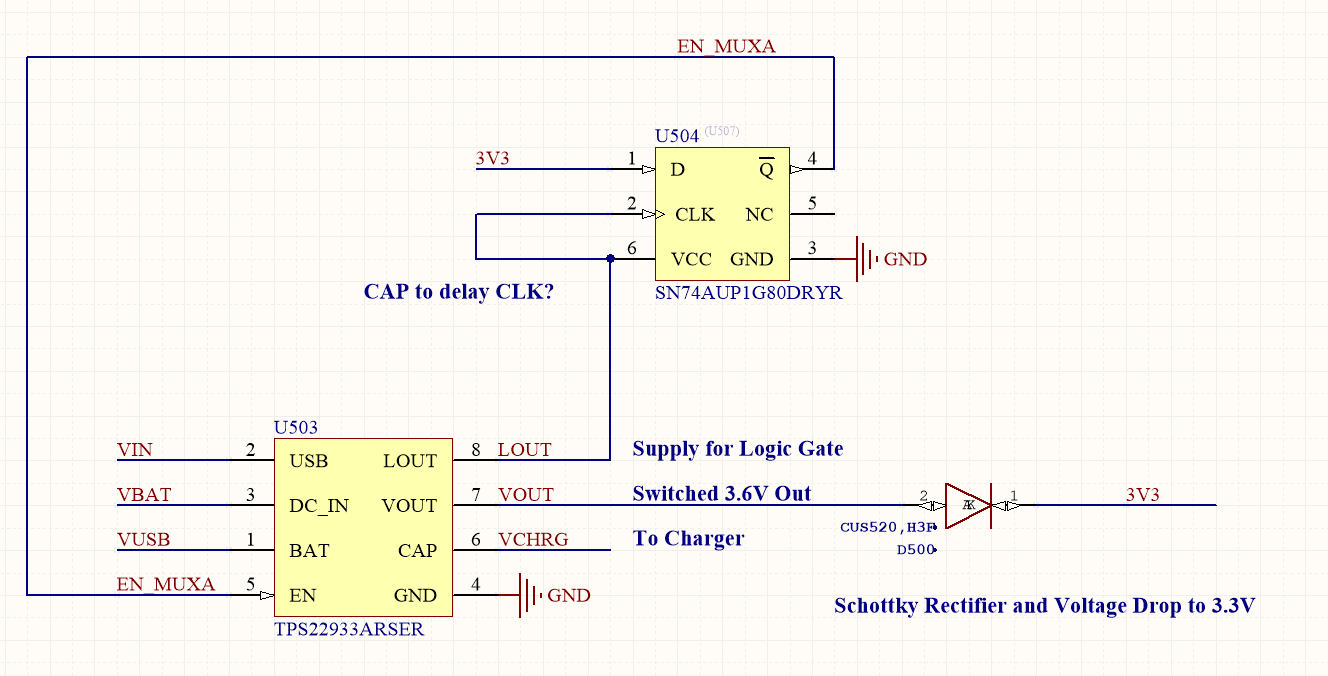
Any rail except 3V3 is powering BQ24040 and charging a small battery (VCHRG in schematic).
VOUT is switched 3V6 dropped via Schottky Diode to about 3.3V and finally feeds 3V3 rail
Well, I guess by now the "circular reference" is already clear: the TPS22933 should only be enabled if 3V3 is absent - but because TPS22933 itself is generating 3V3, that's a problem which can not be fixed with a simple logic inverter (EN = !3V3).
I thought of another power mux, but they will all bringt additional power consumption even if 3V3 is the only source (and additional 10uA would hurt)
So now I'm having a D FF in mind (SN74AUP1G80):
But I wonder if I can directly connect CLK to VCC. Will the gate see it as a rising edge? Or should I add a 100nF cap or so to create a delay?
Two additional "bonus questions":
- Is any of TPS22933's outputs reverse current protected?
- If the battery is the only (or highest-voltage) source, are problems to be expected because TPS22933's cap is connected to BQ24040, charging the battery, and the battery finally feeding VBAT? I hope not, because (from BQ24040's perspective) VIN < VBAT so it should be in standby, correct?


