This thread has been locked.

If you have a related question, please click the "Ask a related question" button in the top right corner. The newly created question will be automatically linked to this question.

TPS65131: EMI/ringing problem on evaluation board

Part Number: TPS65131
Other Parts Discussed in Thread: TPS65130,

Hello,

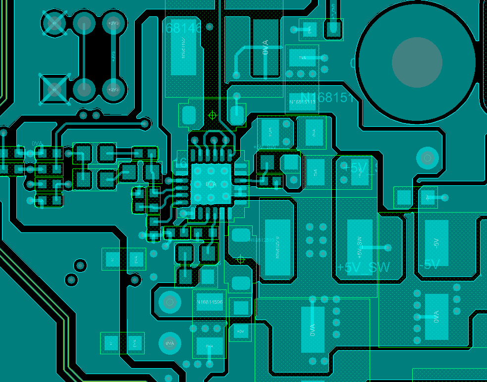
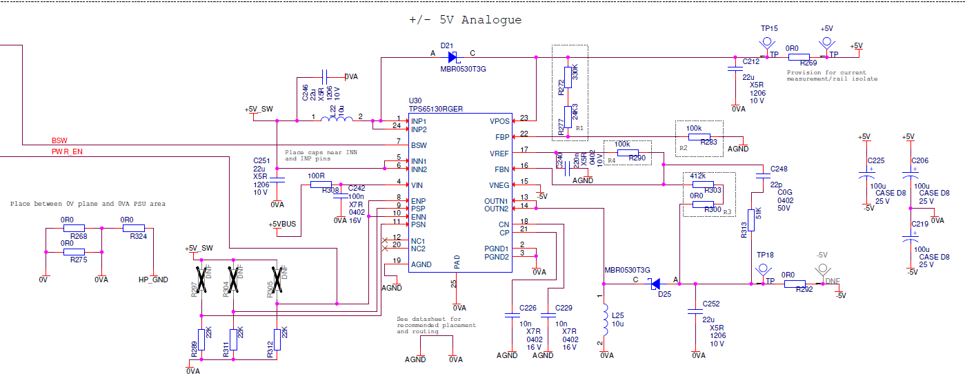
I am currently using a TPS65130 for one of our designs, to generate +/- 5.5V rails (to be exact R300 is actually 47k to have 5.5V, but not relevant for the issue). here schematic of my implementation:

We are currently doing some initial EMI compliance testing and it's failing to pass due to heavy spikes related to this converter.

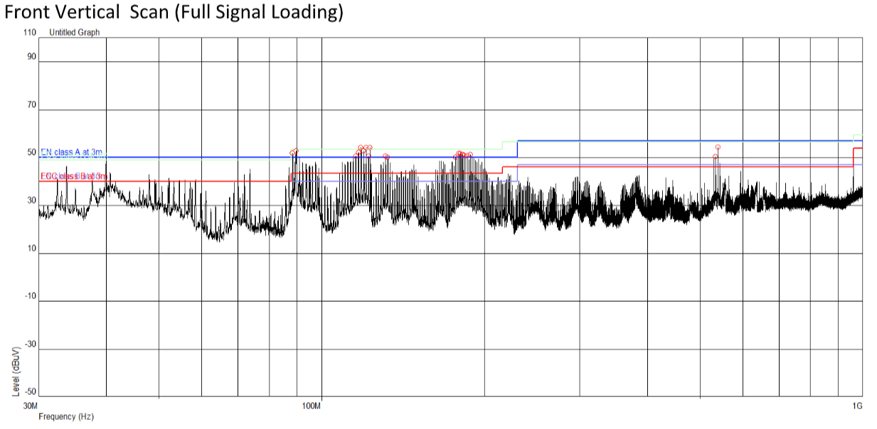
All the spikes in the graph are 1.3 MHz apart, which is the switching frequency of the TPS65130. I can disable the converter and all spikes disappear.

I started investigating by probing the switching nodes for the positive and negative outputs (Pin 13-14 for negative, pin 1-24 for positive). I noticed very high switching spikes on the negative side while switching. The positive spikes are higher than the negative.

I tried changing diodes, changing compensation caps, inductors: no difference at all.

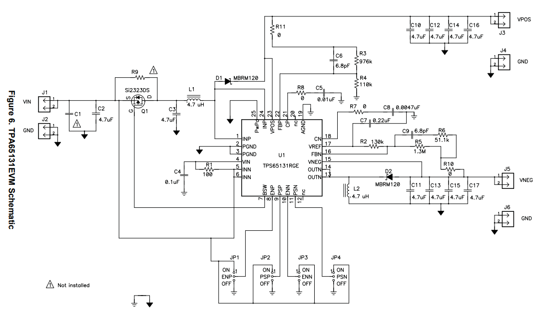
I took a step back and went on the evaluation board TPS6513xEVM-063 (which uses a TPS65131 instead), with all original parts apart from:

- Q1 bypassed

- diodes are now MBR0530T3G

- output voltages set to +/- 5.5V

- connected a 20 ohm resistive load between GND and VNEG output

This is what I get when probing across L2, (DC coupled, 250 MHz BW limit, ground coil around the probe tip):

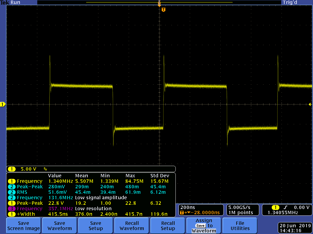
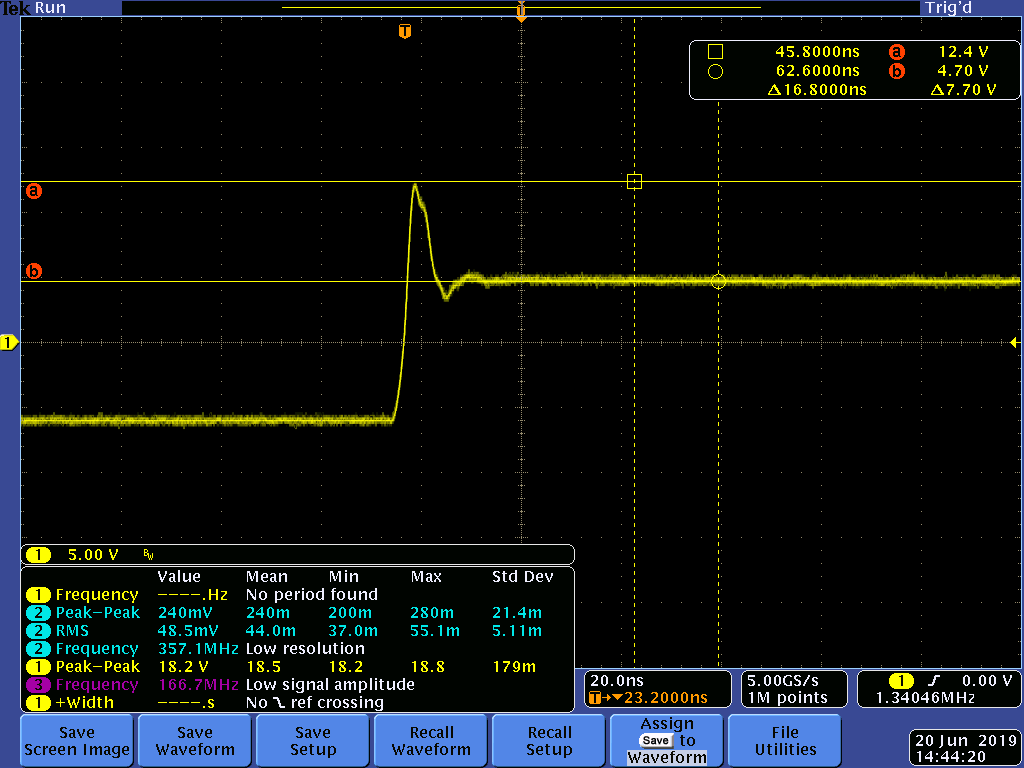
As you can see the positive spike is overshooting by more than 7V. I believe this is the cause of the EMI problem I am experiencing. Given that this behaviour happens already on the evaluation board, it doesn't look promising. 

I tried to add some RC snubbing across the diode OR across the inductor (100pF series with 5 ohm, in both cases), with no difference whatsoever in the result.

Just want to point out that my product scope images look exactly the same, same spikes.

Any recommendation on what to try to fix this? I'd like to see the fix working on the evaluation board first, so please ignore in first instance my implementation.

If there's no way to fix this behaviour we'll be forced to move to another converter/topology as this won't pass regulations.

Many thanks,

Matteo


  • Hi,

    I have notified our expert regarding this topic. Please expect a response by 6/25/19.]

    Thanks,

    Aaron

  • Hi Matteo,

    I'm using the TPS65131 (+15V / -12V outputs) and have also seen large spikes on the eval board. I asked TI about these and they said that the eval board was a typical design, so we moved away from trying to work with it. We improved our layout and managed to reduce our spikes significantly but still needed snubbers on switch nodes to reduce overshoot (20 Ohms and 330pF). That said, we are still a bit concerned as we are slightly violating TI's abs max voltage spec on the switch nodes for <10ns. We tested for emissions without snubbers and passed with a small magin.

    What is your grounding scheme - how have you connected PGND/AGND and thermal pad?

    Can you post plots of your layout?

    Cheers

    Stu

  • Hello Matteo,

    Mitigating EMI in switching converters may require a combination of:

    - layout to reduce high pulsating current loop areas:

    In TPS65131 boost converter for VPOS , high pulsating current loop comprises internal boost switch (pin 1,24), D21 and C212. So the layout should be optimized to reduce this loop area as much as possible.

    For the inverting buck-boost converter in TPS65131, high pulsating current flows through input capacitor C251 through input (pins 5,6), switch internal to the device,D25 and output capacitor C252. Layout should be optimized to reduce the area enclosed by this loop as much as possible.

    - If needed, snubber circuits at SW nodes to reduce ringing and overshoot.

    - high frequency capacitor (0.1uF, 1uf) at the output in addition to bulk capacitance used at the output for reducing ripple: parallel to C212 in the boost converter and parallel to C252 for the inverting buck boost converter.

    - Solid un-interrupted GND plane. In my experience, a single board level ground plane for both signal and power ground is better from EMI perspective than isolated signal and power grounds that connected at one point only.

    I hope that some of these suggestions are helpful. Unfortunately, EMI is system level problem and we can only provide general guidelines. TPS65131EVM board was not targeted for EMI compliance and therefore may not have been optimized from that perspective.

    Kind Regards,

    Liaqat

  • Hi Matteo,

    We have used an uninterrupted ground plane for signal and power on our design. Our TPS65131 AGND and PGNDs are combined close to the device and at the powerPAD under the device. The EVM manual recommends separate analogue and power ground paths, but I think this could be misleading. The data sheet layout recommendations seem to contradict the EVM recommendations. Maybe someone from TI could clarify?

    Regards

    Stu

  • Hi Stu, 

    thanks for your answer. 

    Here's a screenshot of my layout:

    Board is 4 layers, this is the bottom. Next layer up in purple: 

    Next layer up in green:

    Last (and top layer) in red:

    As you can see, it's quite similar to the eval board layout.

    Do you get similar rising overshoot on your board? Would you be able to post an example of your layout? 

    You mentioned that your board is passing just about the emissions test without snubber. Is the situation improved (EMC wise) by adding the snubber? In our case there was no significant difference.

    Does the frequency plot from your device looks similar to ours? lots of spikes 1.3 MHz apart from each other?

    Many thanks,

    Matteo

  • Hi Matteo,

    We got about 4V overshoot on switch nodes only on a previous layout but reduced it significantly with our second attempt to about 1V. Keep in mind our outputs are +15V and -12V from +5V in. Our 15V and -12V rails were pretty solid.

    We have seven switchers on our board and our emissions looked similar to yours - we modified our layout for other switchers too and this got us a pass. We have yet to re-evaulate EMI with snubbers and gate resistors to see if we can improve on things. All we've ascertained so far is that the high-current AC switching loops (hot loops) on our design were our main problem. We do expect further improvements as a result of reducing the ringing on switch nodes, though.

    I'll post some layout later, but you can see a plot on another thread where we have a problem: 'Abnormal overshoot on positive 15V rail'

    Cheers

    Stew

  • Hello,

    any recommendation where to put the snubbers?

    I've been trying so far to put them across the diodes with little change over the resulting spike.

    Would it make any sense to place them across the negative inductor instead?

    Thanks

  • We saw significant overshoot reduction on switch nodes (OUTN to 0V and INP to 0V) with 20R & 330pF(470pF max).

    Stew

  • Keep an eye on power dissipation in the snubbers

  • Thanks, I'll try that!