This thread has been locked.

If you have a related question, please click the "Ask a related question" button in the top right corner. The newly created question will be automatically linked to this question.

UCC28180: UCC28180 failure issue

Part Number: UCC28180

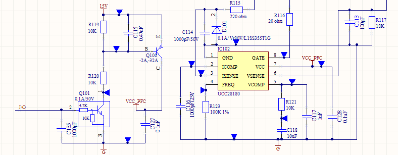
We have encountered one issue on the UCC28180 which was used in our production at our lab. The PF value became very low and the waveform was distorted.

The distorted waveform:

The normal waveform:

From the Gate PWM output waveform, we can see the abnormal performance on the position of the distorted waveform. Could you give us some possible failure reason. Thanks!

Follow is the sch:

  • ,

    What were the test conditions when you captured this waveform and what is the design specification for your requirements?

    Did you use the Excel calculator ?

    If so can you please attach the results ?

    Regards

    John

  • The test condition is : normal operating  with the power about 3KW.  The load is  BLDC motor.

    I did use the calculator. Please check it as below:

    INPUT:
    Minimum Input Voltage from AC Line: VACIN(min) 176 VRMS
    Maximum Input Voltage from AC Line: VACIN(max) 265 VRMS
    Minimum Line Frequency: fLINE(min): 47 Hz
    Maximum Line Frequency: fLINE(max): 63 Hz
    Minimum Rectified AC Line Voltage: VIN_PEAK(min) 248.902 V
    Maximum Rectified AC Line Voltage: VIN_PEAK(max) 374.767 V
     
    OUTPUT:
    Maximum Output Power of PFC Stage: POUT(max) 6000 W
    Output Voltage (Note: Must be > VIN_RECTIFIED(max)): VOUT 375 V
    Target Power Factor, VIN(nom), Full Load: PF 0.99  
    Predicted Efficiency: h 0.9  
    Maximum Ambient Temperature: TAMB(max) 50 °C
    Maximum Average Output Current of PFC Stage: IOUT 16.000 A
    Desired Switching Frequency: fSW(target) 22 kHz
    Recommended Resistor value on FREQ to Set the Switching Frequency, fSW: RFREQ(recommended) 105.000 kΩ
    Actual Value For RFREQ Used:  RFREQ = 100
    Resultant Switching Frequency, fSW: fSW 22.640 kHz
           
           
    Line Current:
    Maximum Input Power Drawn from the Line: PIN(max) 6666.667 W
    Maximum RMS AC Line Current: IIN_RMS(max) 38.261 A
    Maximum Peak AC Line Current, assuming sinusoidal: IIN_PEAK(max) 54.110 A
    Maximum Average AC Line Current, assuming sinusoidal: IIN_AVG(max) 34.447 A
    Minimum Input Fuse Rating: IFUSE 57.392 A
     
    BRIDGE RECTIFIER:
    Bridge Rectifier Forward Voltage, at IIN_PEAK(max): VF_BRIDGE 1 V
    Bridge Rectifier Thermal Resistance, Junction to Case: RqJC(Bridge) 2.2 °C/W
    Case to Heatsink Thermal Resistance: RθCHS(Bridge) 0.61 °C/W
    Bridge Rectifier Maximum Junction Temperature: TJ(max) 125 °C
    Bridge Rectifier Minimum Average Current Rating: IBRIDGE(rated) 51.671 A
    Bridge Rectifier Minimum DC Blocking Voltage Rating: VDC_BLOCKING(rated) 412.243 V
    Bridge Rectifier Power Dissipation: PBRIDGE 68.895 W
    Required Heat Sink Thermal Impedance: RqHS_AMB(Bridge) -1.721 °C/W
     
    INPUT CAPACITOR:
    Inductor Peak-to-Peak Current Ripple Factor (i.e. 0.2 for 20%, 0.3 for 30%). Percentage of minimum input, maximum load, inductor current at 50% duty cycle operating point, not recommended to be > 0.4: LI_ripple_factor(target) 0.3  
    Maximum High Frequency Voltage Ripple Factor (i.e. 0.03 for 3%, 0.09 for 9%): VCin_ripple_factor 0.07  
    Target Maximum Allowable Inductor Current Ripple: IRIPPLE(target) 16.233 A
    Maximum Inductor Voltage Ripple: VIN_RIPPLE 17.423 V
    Recommended Input Capacitor Value: CIN(recommended) 4.700 mF
    Actual Value of Input Capacitor Used: CIN 0.330 µF
    Required Minimum Voltage Rating for CIN: VCIN(rating) 412.243 V
     
    BOOST INDUCTOR DESIGN:
    Maximum Duty Cycle: DUTY(max) 0.336  
    Maximum Inductor Peak Current: IL_PEAK(max) 62.226 A
    Minimum Recommended Boost Inductor Value: LBST(recommended) 0.255 mH
    Actual Boost Inductor Value Used: LBST(actual) = 0.5 mH
    Actual Maximum Inductor Ripple Current: IRIPPLE(actual) 8.282 A
    Actual Maximum Inductor Peak Current: IL_PEAK(actual) 58.251 A
    Resultant Inductor Current Ripple Factor: LI_ripple_factor(actual) 0.153  
     
    BOOST DIODE:
    Forward Voltage Drop, at IL_PEAK(max),125°C: VF 1 V
    Reverse Recovery Charge: QRR 0 nC
    Boost Diode Maximum Junction Temperature: TJ(max) 125 °C
    Boost Diode Thermal Resistance, Junction to Case: RqJC(Diode) 1.5 °C/W
    Boost Diode Thermal Resistance, Case to Heatsink: RqCHS(Diode) 0.32 °C/W
    Boost Diode Conduction Losses: PDIODE(cond) 16.000 W
    Reverse Recovery Losses: PREVERSE 0.000 W
    Total Boost Diode Losses: PDIODE(total) 16.000 W
    Required Heat Sink Thermal Impedance: RqHS_AMB(Diode) 2.868 °C/W
    Required Diode Blocking Voltage: VBLOCKING 412.500 V
     
    SWITCHING ELEMENT:
    VCC Bias Voltage to the UCC28180: VCC 16 V
    Gate-Source Voltage: VGS 15.2 V
    Drain-Source RMS Current: IDS_RMS 22.526 A
    FET On-Resistance at  TJ = 125°C:  RDSon 0.35 W
    FET Gate Charge at VGS: Qg 87 nC
    FET Rise Time: tr 5 ns
    FET Fall Time: tf 4.5 ns
    FET Output Capacitance: COSS 780 pF
    FET Maximum Junction Temperature: TJ(max) 125 °C
    FET Thermal Resistance, Junction to Case: RqJC(FET) 0.61 °C/W
    FET Thermal Resistance, Case to Heatsink: RqCHS(FET) 0.32 °C/W
    Gate Drive Losses (actually dissipated in the gate drive circuitry): PGATE 0.030 W
    FET Conduction Losses: PCOND 177.595 W
    FET Switching Losses: PSW 3.424 W
    FET Losses, Total: PFET 181.019 W
    Required Heat Sink Thermal Impedance: RqHS_AMB(FET) -0.516 °C/W
     
    CURRENT SENSE RESISTOR:
    Ideal Value for RSENSE, for 110% Inductor SOC Threshold: RSENSE(ideal) 0.004 W
    Actual Value for RSENSE: Current Sense Resistor: RSENSE 0.003 W
    Inductor Current at Soft Over-Current Threshold: IOVERCURRENT_SOC 86.333 A
    Power Dissipated in RSENSE: PRsense 4.392 W
    Theoretical Output Over-Current Inception Point: IOUT_OVERCURRENT 24.435 A
    Maximum ISENSE Peak Current Limit Threshold: IPCL 146.000 A
    Resistance of Thermistor at 25°C: RTHERM 5 W
    Maximum Inrush Current: IINRUSH 74.953 A
    Recommended ISENSE Series Resistor: RISENSE 220 W
    Recommended ISENSE Filter Capacitor: CISENSE 3900 pF
     
    OUTPUT CAPACITOR:
    Required Minimum Output Voltage: VOUT_HOLDUP(min) 280 V
    Desired Number of Line Cycles For Output Holdup Time  (typ one line cycle): NHOLD_UP 1  
    Minimum Output Voltage Holdup Time: tHold_UP(min) 21.277 ms
    Recommended Minimum Output Capacitor Value: COUT(recommended) 3900.000 µF
    Actual Output Capacitor Value: COUT 2790 µF
    Output Voltage Peak to Peak Ripple: VOUT_RIPPLEpp 9.710 V
    Good! Output voltage peak-peak ripple is less than 5% VOUT
    Output Capacitor Ripple Current at Twice Line Frequency: ICout_2fline 11.314 ARMS
    Output Capacitor High Frequency Ripple Current: ICout_HF 16.455 ARMS
    Total Output Capacitor Ripple Current: ICout_RMS(total) 19.969 ARMS
     
    OUTPUT VOLTAGE SET POINT:
    Recommended Value for the Top Divider Resistor: RFB1(recommended) 1 MW
    Actual Value of the Top Divider Resistor: RFB1(actual) 1.32 MW
    Recommended Value for the Bottom Divider Resistor (E48 Series): RFB2(recommended) 17.800 kW
    Actual Value of the Bottom Divider Resistor: RFB2(actual) 18 kW
    Actual Nominal Output Voltage: VOUT 371.667 V
    Minimum Output Voltage with respect to VREF: VOUT(min) 366.463 V
    Maximum Output Voltage with respect to VREF: VOUT(max) 376.870 V
    OVP Set Point: Typical DC Output Voltage to Trigger OVP: VOVP 405.117 V
    UVD Set Point: Typical DC Output Voltage to Trigger UVD: VUVD 353.083 V
    Recommended Value for Filter Capacitor on VSENSE: CVSENSE 560.000 pF
    Power Dissipated in Voltage Divider: PRfB1+RFB2 0.103 W
    DO NOT PROCEED UNTIL RFB2 IS DECREASED SO MINIMUM OUTPUT VOLTAGE > MAXIMUM RECTIFIED INPUT VOLTAGE
    COMPENSATION:


    The Loop will be Optimized at a Selected Specific Line Voltage.  For a Wide Input Range, Optimization is Recommended at the Mean of Min and Max Input.  For a Design with a Specific Nominal Line Voltage, Optimize at that Nominal Voltage. VCOMP at Any Line Voltage or as a Function of Load is Shown at Right
    Line Voltage for Optimized Loop Design: VINnom 220.5 V
    Open Loop Transfer Function for Current Loop:  
    Product of the Voltage Loop Variables: M1M2 0.060 V/ms
    VCOMP Voltage at VINnom: VCOMP 2.457 V
    Internal Current Loop Gain Factor M1: M1 0.368  
    Internal Voltage Loop PWM Ramp Slope M2: M2 0.163 V/ms
    Non-Linear Gain Voltage Loop Variable M3: M3 0.112 V/ms
    Maximum Recommended ICOMP Capacitor Value: CICOMPmax(recommended) 0.015 µF
    Minimum Recommended ICOMP Capacitor Value: CICOMPmin(recommended) 6800.000 0
    Actual Value Used for ICOMP Capacitor: CICOMP(actual) 1000 pF
    Resultant Actual Current Averaging Pole Frequency: fIAVG(actual) 7.949 kHz


    Open Loop Transfer Function for Voltage Loop:  
    PWM to Power Stage Pole: fPWM_PS(pole) 2.729 Hz
    Desired Voltage Loop Crossover Frequency ( fV < 20Hz): fV 8 Hz
    Open Loop Voltage Gain at Desired fV: GVLdB(fV) 9.607 dB
    Recommended Value for the Voltage Compensation Capacitor: CVCOMP(recommended) 10.000 µF
    Actual Value Used for CVCOMP Capacitor: CVCOMP(actual) 10 mF
    Recommended Value for the Voltage Compensation Resistor: RVCOMP(recommended) 5.900 kW
    Actual Value Used for RVCOMP Resistor: RVCOMP(actual) 10 kW
    Resultant Value of Voltage Compensation Zero: fZERO 1.592 Hz
    Desired Voltage Compensation Pole (fPole < 50Hz): fPOLE 18 Hz
    Recommended Value for the Parallel Voltage Compensation Capacitor: CVCOMP_P(recommended) 1.000 µF
    Actual Value for the Parallel Voltage Compensation Capacitor: CVCOMP_P(actual) 1 mF

    INPUT:
    Minimum Input Voltage from AC Line: VACIN(min) 176 VRMS
    Maximum Input Voltage from AC Line: VACIN(max) 265 VRMS
    Minimum Line Frequency: fLINE(min): 47 Hz
    Maximum Line Frequency: fLINE(max): 63 Hz
    Minimum Rectified AC Line Voltage: VIN_PEAK(min) 248.902 V
    Maximum Rectified AC Line Voltage: VIN_PEAK(max) 374.767 V
     
    OUTPUT:
    Maximum Output Power of PFC Stage: POUT(max) 6000 W
    Output Voltage (Note: Must be > VIN_RECTIFIED(max)): VOUT 375 V
    Target Power Factor, VIN(nom), Full Load: PF 0.99  
    Predicted Efficiency: h 0.9  
    Maximum Ambient Temperature: TAMB(max) 50 °C
    Maximum Average Output Current of PFC Stage: IOUT 16.000 A
    Desired Switching Frequency: fSW(target) 22 kHz
    Recommended Resistor value on FREQ to Set the Switching Frequency, fSW: RFREQ(recommended) 105.000 kΩ
    Actual Value For RFREQ Used:  RFREQ = 100
    Resultant Switching Frequency, fSW: fSW 22.640 kHz
           
           
    Line Current:
    Maximum Input Power Drawn from the Line: PIN(max) 6666.667 W
    Maximum RMS AC Line Current: IIN_RMS(max) 38.261 A
    Maximum Peak AC Line Current, assuming sinusoidal: IIN_PEAK(max) 54.110 A
    Maximum Average AC Line Current, assuming sinusoidal: IIN_AVG(max) 34.447 A
    Minimum Input Fuse Rating: IFUSE 57.392 A
     
    BRIDGE RECTIFIER:
    Bridge Rectifier Forward Voltage, at IIN_PEAK(max): VF_BRIDGE 1 V
    Bridge Rectifier Thermal Resistance, Junction to Case: RqJC(Bridge) 2.2 °C/W
    Case to Heatsink Thermal Resistance: RθCHS(Bridge) 0.61 °C/W
    Bridge Rectifier Maximum Junction Temperature: TJ(max) 125 °C
    Bridge Rectifier Minimum Average Current Rating: IBRIDGE(rated) 51.671 A
    Bridge Rectifier Minimum DC Blocking Voltage Rating: VDC_BLOCKING(rated) 412.243 V
    Bridge Rectifier Power Dissipation: PBRIDGE 68.895 W
    Required Heat Sink Thermal Impedance: RqHS_AMB(Bridge) -1.721 °C/W
     
    INPUT CAPACITOR:
    Inductor Peak-to-Peak Current Ripple Factor (i.e. 0.2 for 20%, 0.3 for 30%). Percentage of minimum input, maximum load, inductor current at 50% duty cycle operating point, not recommended to be > 0.4: LI_ripple_factor(target) 0.3  
    Maximum High Frequency Voltage Ripple Factor (i.e. 0.03 for 3%, 0.09 for 9%): VCin_ripple_factor 0.07  
    Target Maximum Allowable Inductor Current Ripple: IRIPPLE(target) 16.233 A
    Maximum Inductor Voltage Ripple: VIN_RIPPLE 17.423 V
    Recommended Input Capacitor Value: CIN(recommended) 4.700 mF
    Actual Value of Input Capacitor Used: CIN 0.330 µF
    Required Minimum Voltage Rating for CIN: VCIN(rating) 412.243 V
     
    BOOST INDUCTOR DESIGN:
    Maximum Duty Cycle: DUTY(max) 0.336  
    Maximum Inductor Peak Current: IL_PEAK(max) 62.226 A
    Minimum Recommended Boost Inductor Value: LBST(recommended) 0.255 mH
    Actual Boost Inductor Value Used: LBST(actual) = 0.5 mH
    Actual Maximum Inductor Ripple Current: IRIPPLE(actual) 8.282 A
    Actual Maximum Inductor Peak Current: IL_PEAK(actual) 58.251 A
    Resultant Inductor Current Ripple Factor: LI_ripple_factor(actual) 0.153  
     
    BOOST DIODE:
    Forward Voltage Drop, at IL_PEAK(max),125°C: VF 1 V
    Reverse Recovery Charge: QRR 0 nC
    Boost Diode Maximum Junction Temperature: TJ(max) 125 °C
    Boost Diode Thermal Resistance, Junction to Case: RqJC(Diode) 1.5 °C/W
    Boost Diode Thermal Resistance, Case to Heatsink: RqCHS(Diode) 0.32 °C/W
    Boost Diode Conduction Losses: PDIODE(cond) 16.000 W
    Reverse Recovery Losses: PREVERSE 0.000 W
    Total Boost Diode Losses: PDIODE(total) 16.000 W
    Required Heat Sink Thermal Impedance: RqHS_AMB(Diode) 2.868 °C/W
    Required Diode Blocking Voltage: VBLOCKING 412.500 V
     
    SWITCHING ELEMENT:
    VCC Bias Voltage to the UCC28180: VCC 16 V
    Gate-Source Voltage: VGS 15.2 V
    Drain-Source RMS Current: IDS_RMS 22.526 A
    FET On-Resistance at  TJ = 125°C:  RDSon 0.35 W
    FET Gate Charge at VGS: Qg 87 nC
    FET Rise Time: tr 5 ns
    FET Fall Time: tf 4.5 ns
    FET Output Capacitance: COSS 780 pF
    FET Maximum Junction Temperature: TJ(max) 125 °C
    FET Thermal Resistance, Junction to Case: RqJC(FET) 0.61 °C/W
    FET Thermal Resistance, Case to Heatsink: RqCHS(FET) 0.32 °C/W
    Gate Drive Losses (actually dissipated in the gate drive circuitry): PGATE 0.030 W
    FET Conduction Losses: PCOND 177.595 W
    FET Switching Losses: PSW 3.424 W
    FET Losses, Total: PFET 181.019 W
    Required Heat Sink Thermal Impedance: RqHS_AMB(FET) -0.516 °C/W
     
    CURRENT SENSE RESISTOR:
    Ideal Value for RSENSE, for 110% Inductor SOC Threshold: RSENSE(ideal) 0.004 W
    Actual Value for RSENSE: Current Sense Resistor: RSENSE 0.003 W
    Inductor Current at Soft Over-Current Threshold: IOVERCURRENT_SOC 86.333 A
    Power Dissipated in RSENSE: PRsense 4.392 W
    Theoretical Output Over-Current Inception Point: IOUT_OVERCURRENT 24.435 A
    Maximum ISENSE Peak Current Limit Threshold: IPCL 146.000 A
    Resistance of Thermistor at 25°C: RTHERM 5 W
    Maximum Inrush Current: IINRUSH 74.953 A
    Recommended ISENSE Series Resistor: RISENSE 220 W
    Recommended ISENSE Filter Capacitor: CISENSE 3900 pF
     
    OUTPUT CAPACITOR:
    Required Minimum Output Voltage: VOUT_HOLDUP(min) 280 V
    Desired Number of Line Cycles For Output Holdup Time  (typ one line cycle): NHOLD_UP 1  
    Minimum Output Voltage Holdup Time: tHold_UP(min) 21.277 ms
    Recommended Minimum Output Capacitor Value: COUT(recommended) 3900.000 µF
    Actual Output Capacitor Value: COUT 2790 µF
    Output Voltage Peak to Peak Ripple: VOUT_RIPPLEpp 9.710 V
    Good! Output voltage peak-peak ripple is less than 5% VOUT
    Output Capacitor Ripple Current at Twice Line Frequency: ICout_2fline 11.314 ARMS
    Output Capacitor High Frequency Ripple Current: ICout_HF 16.455 ARMS
    Total Output Capacitor Ripple Current: ICout_RMS(total) 19.969 ARMS
     
    OUTPUT VOLTAGE SET POINT:
    Recommended Value for the Top Divider Resistor: RFB1(recommended) 1 MW
    Actual Value of the Top Divider Resistor: RFB1(actual) 1.32 MW
    Recommended Value for the Bottom Divider Resistor (E48 Series): RFB2(recommended) 17.800 kW
    Actual Value of the Bottom Divider Resistor: RFB2(actual) 18 kW
    Actual Nominal Output Voltage: VOUT 371.667 V
    Minimum Output Voltage with respect to VREF: VOUT(min) 366.463 V
    Maximum Output Voltage with respect to VREF: VOUT(max) 376.870 V
    OVP Set Point: Typical DC Output Voltage to Trigger OVP: VOVP 405.117 V
    UVD Set Point: Typical DC Output Voltage to Trigger UVD: VUVD 353.083 V
    Recommended Value for Filter Capacitor on VSENSE: CVSENSE 560.000 pF
    Power Dissipated in Voltage Divider: PRfB1+RFB2 0.103 W
  • Please test your circuit with a resistive load.

    It may be that your BLDC load is non-linear and causing the strange waveform on the input.

    What were the test conditions for your so-called "normal"  and "distorted" waveforms ?

    Regards

    John