Other Parts Discussed in Thread: CSD17313Q2Q1, TPS51216, TPS51916
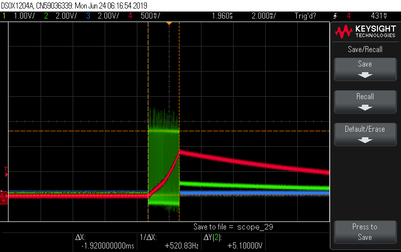
I have three boards from the same batch that implement the application circuit from the datasheet to power two DDR3L chips (1.35V). One of the boards can power-up and has a seemingly stable output. The other two boards fail to stabilize and appear to latch into either the OVP or UVP state, depending on how much load capacitance. In one case the output goes up to 1.5V before it shuts off. Here is a plot that shows the SW (green) and VDDQ (red). After 2ms from the start of SMPS operation, the output fails to reach REFIN (1.35V) and latches off.
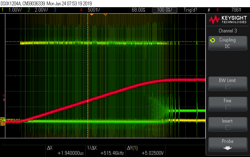
On this one the load capacitance is reduced by 20uF, but then the output voltage goes over 1.35V and again the switching stops. One observation is that the SW output doesn't go to zero, which should happen according to datasheet after an OVP fault: "When an OV event is detected, the controller latches DRVH low and DRVL high."
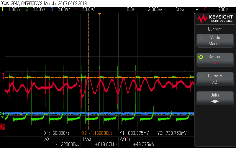
Red = VDDQ
Blue = REFIN
Green = SW

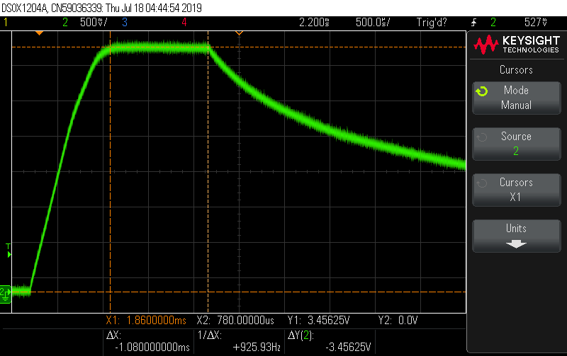
Here is a view of the board that is able to regulate:
Some observations:
1. The failing boards have the oddly shaped VDDQ waveform that looks a power function instead of a linear or negative exponential. The 'good' board has a linear ramp.
2. The switching frequency is all over the place. The failing boards are pretty consistently hammering the FETs at about 600kHz. Much higher than I imagined since it's set for 400kHz. The 'good' board even has some pulses that are in the MHz range. Is that normal at startup or should it really be no faster than 400kHz all the time (except in light-load)?
3. The 'good' board appears to throttle back on the pulses, while the failing boards have a very constant frequency (even though it's way too fast) up until it latches off from OVP or UVP. Why isn't the chip seeing the high voltage and throttling back?
Is this a stability issue?