This thread has been locked.

If you have a related question, please click the "Ask a related question" button in the top right corner. The newly created question will be automatically linked to this question.

LM5060: Backfeed from VOUT coming back through OUT / GATE

Part Number: LM5060

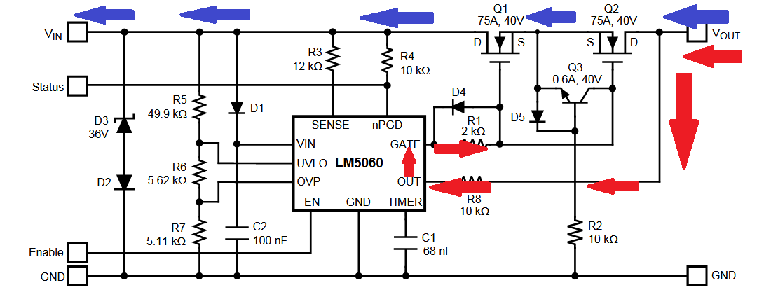
I am using the LM5060 in a circuit configuration similar to Figure 41 of the datasheet.  In our application, I have another circuit that can backfeed battery voltage to VOUT.  It is possible also for this condition to occur in our end-application when VIN is unpowered.  The resulting issue is that the battery voltage that is backfed to VOUT is coming back out of VIN as well, which is not desired.  It appears this is occurring by VOUT backfeeding into the LM5060 OUT pin, through the internal diode (shown in the functional block diagram of Section 7.2 of datasheet), and back out the GATE (red arrows).  Somehow, this gate voltage is high enough to partially turn on the MOSFETs which results in that voltage being present at VIN (blue arrows) and able to drive some significant current.

What is the best way to mitigate this issue?  Would one potential solution be to connect OUT through a resistor to the common source of Q1/Q2 instead of the drain of Q2?  Are there other options?

  • Hi Bryan,

    Thanks for reaching us on E2E.

    I will go through it and reply by end of the day tomorrow. 

    Best Regards,

    Rakesh

  • Hi Bryan,

    Your image attachments are missing. Can you please re-post them.

    From your understanding, it looks like the problem is due to reverse current blocking. The configuration in Figure 41 blocks reverse current only when the controller is OFF. To avoid this, you would need true reverse current blocking solution such as Ideal diode controller + hot-swap controller (please refer http://www.ti.com/tool/tida-00233)

    Best Regards,

    Rakesh

  • Hi Rakesh,

    Thanks for the quick response.  I am re-attaching the image, hoping it comes through this time.

    Based on the response, I am not sure I explained our issue clearly, so will try to re-explain.  This condition exists with the device commanded to an 'off' state, and we are not actively providing voltage to VIN (e.g. battery voltage removed in the system - e.g. switched battery).

    In our design, there are other circuits that can backfeed to VOUT (as labeled in Figure 41).  When this occurs, along with the LM5060 commanded 'off' and no voltage provided by our system to VIN, it appears the voltage at VOUT backfeeds into LM5060 OUT pin, through the internal diode shown in block diagram of Section 7.2 datasheet, and out of the GATE pin.  The resultant voltage that is fed through the LM5060 to the OUT pin is high enough to turn on the FET in its linear region.  This then provides an unintended path from VOUT to VIN, which is not desired.

    If I remove R8 of Figure 41, the issue goes away, so the path is confirmed to be in to the OUT pin and back through the GATE with the GATE voltage capable of turning on the N-FETs.  If I move the connection point of R8 to the common source of the back-to-back FETs instead of VOUT, the issue goes away as well, due VOUT being unable to get to that node, thus no backfeed to OUT.  Are there any concerns in doing this?

    Thanks,
    Bryan

  • Hi Bryan,

    Thanks for sending it again and explanation.  Yes, you can change connection point of R8 to the common source of the back-to-back FETs (like Figure-1 in http://www.ti.com/lit/an/snva683/snva683.pdf) to overcome the problem. This will not cause any issue. 

    Best Regards,

    Rakesh