This thread has been locked.

If you have a related question, please click the "Ask a related question" button in the top right corner. The newly created question will be automatically linked to this question.

TPS54325: About IC burns on short between VIN and VBST pins on TPS54325.

Part Number: TPS54325

Dear support member,

The customer is mass producing the TPS54325.

I have a question and Urgent.
The IC burned due to a short between the VIN(13pin) and VBST(12pin) pins.

(Question)
Q1
Please tell me the mechanism by which the IC burns.


(Specification condition)
Vin: 12V
Vout: 3.3V
Iout: 1.8A

Best regard.
Bob Lee.

  • Hi,

    Because the bootstrap circuit between VBST and SW only works below 6.5V (see Page 4 & 8 of its datasheet), if the voltage exceeds it, the device might burn. Thanks.

  • Dear Iven Su,

    Thank you very much for your answer.
    I understood about VBST and SW absolute max voltage.

    May I ask add a question?

    Question 2
    Could you teach the mechanism that damages the IC?
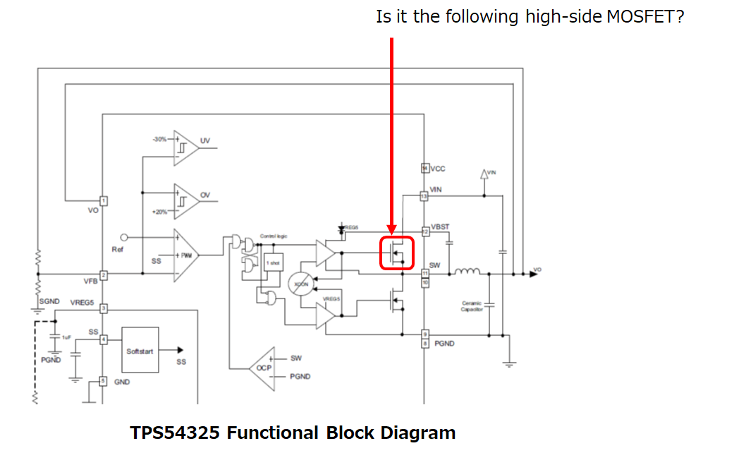
    Please describe in the internal block diagram and tell me.

    Best regard.
    Bob Lee.

  • Hi,

    The voltage higher than absolute max voltage will damage the low-voltage FETs which used in bootstrap circuit. Vin voltage exceeds these max drain-source voltage of these FETs, so the FETs will burn. So driver of high-side switch now is damaged and the device will not work. Thanks.

  • Dear Iven Su,

    Thank you very much for your answer.
    May I ask a add question about your answer?


    About Question
    (Your answer)
    So your answer that "The voltage higher than absolute max voltage will damage the low-voltage FETs which used in bootstrap circuit. "


    Question4
    Is this the low-voltage FETs a high side MOSFET?
    Is it the following high-side MOSFET?


    About Question
    (Your answer)
    So your answer that "Vin voltage exceeds these max drain-source voltage of these FETs, so the FETs will burn. "

    Question5
    Is there the absolute maximum voltage rating drain-source voltage of a High-side MOSFET?(VIN-SW absolute maximum voltage rating )?

    Is there description of datasheet?


    Because I don't understand "Vin voltage exceeds these max drain-source voltage of these FETs".


    Best regard.
    Bob Lee.

  • Hi,

    Answer to Q4: The MOSFET you marked out is high-side power switch, and the low-voltage FETs mentioned above are logic switches, which are basic units of control/driver circuits of the device.

    Answer to Q5: These low-voltage FETs in bootstrap circuit part have 6.5Vmax, and High-side power MOSFET is 20Vmax, thanks.

  • Dear Iven Su,


    Thank you very much for your answer.
    I reply my customer your answer.

    I will feedback my cusomter status.

    Best regard.
    Bob Lee.

  • Dear Iven Su,

    Thank you very much for support.
    My customer solved.

    Best regard.
    Bob Lee.