Hello E2E,
We found double pulse at no load/light load.
Is it normal?
if yes, could you please explain the reason?
If not, how to improve it?
<Zoom-in>
<Zoom out>
<Schematic>
BR,
Jason
This thread has been locked.
If you have a related question, please click the "Ask a related question" button in the top right corner. The newly created question will be automatically linked to this question.
Hi,
It could be that you are at the minimum on time of the device? Is this happen at lower input voltage too?
Could you lower the frequency by changing the R1174 to 100kohm
Thanks
-Arief
Arief,
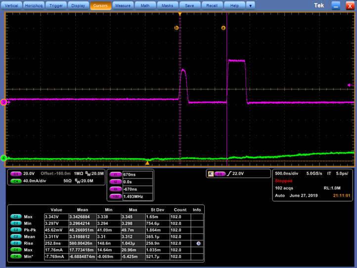
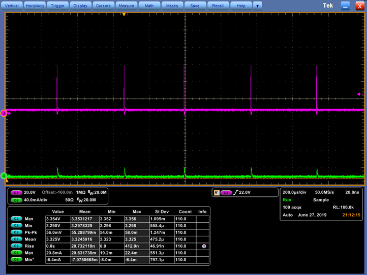
Eliminate the double pulse is not our main purpose and input voltage is fixed. we just want to know the reason and if it will impact the system stability or not.
The timing of the first pulse is close to the minimum ON time.
How come caused the minimum on time at no load and it is regular appear minimum ON time followed by normal switching pulse?
BR,
Jason
Arief,
Beside to the question above, we also want to know the high side FET Vds voltage stress.
In one of test item, we need to verify high side FET peak voltage, but we didn't find the spec in datasheet.
please advise.
BR,
Jason
Hi Jason,
Sorry for the delay in response
In terms of high side FET peak voltage, I would recommend not exceeding the abs max of 65V. I believe this is what it is tested.
As for double pulse, the first initial pulse could be from the charging of the boot capacitor through the SW node at this light load condition.
You should resume to normal pulses when you increase the load current and operate in CCM and fixed frequency
Thanks and I hope that helps
-Arief
Ariel,
What is the maximum voltage stress of high side FET in transient or AC spike?
What is the maximum duration?
BR,
Jason
Hi Jason,
Based on the datasheet the abs max for VIN to GND and SW to GND is 65V, therefore i would keep the voltages on this node below this level.
If there is a high spike at the SW node, i would suggest using a snubber to damp the spike.
Thanks
-Arief