


Hi,
Find the attached schematic.
Red mentioned area component we are soldered,
and given external +12V dc supply in D3 anode pin.
Output PIn 7 is 0V, Not getting PWM pulses.
Kindly suggest what will do next.
Regards,
Sathishkumar.
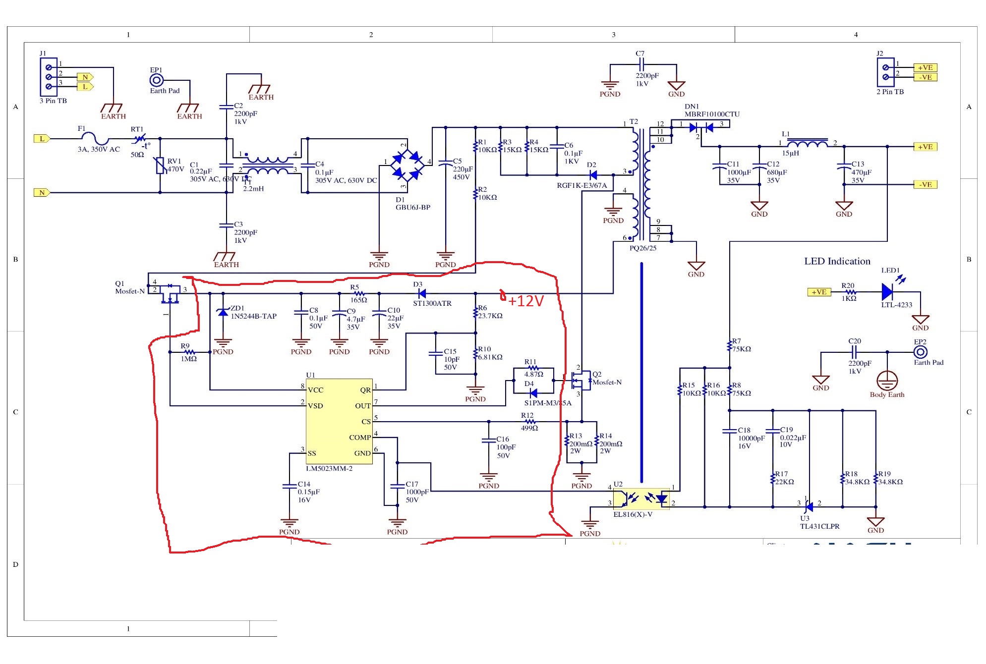
Hi,
Find the attached schematic.
Red mentioned area component we are soldered,
and given external +12V dc supply in D3 anode pin.
Output PIn 7 is 0V, Not getting PWM pulses.
Kindly suggest what will do next.
Regards,
Sathishkumar.
